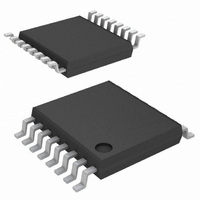
DG612AEQ-T1-E3 Vishay, DG612AEQ-T1-E3 Datasheet - Page 9

DG612AEQ-T1-E3
Manufacturer Part Number
DG612AEQ-T1-E3
Description
1 PC Charge Injection,Quad SPST Switches
Manufacturer
Vishay
Datasheet
1.DG613AEN-T1-E4.pdf
(11 pages)
Specifications of DG612AEQ-T1-E3
Function
Switch
Circuit
4 x SPST - NO
On-state Resistance
72 Ohm
Voltage Supply Source
Single, Dual Supply
Voltage - Supply, Single/dual (±)
2.7 V ~ 12 V, ± 2.7 V ~ 5 V
Current - Supply
1µA
Operating Temperature
-40°C ~ 125°C
Mounting Type
Surface Mount
Package / Case
16-TSSOP
Number Of Switches
Quad
Switch Configuration
SPST
On Resistance (max)
235 Ohm @ 3 V
On Time (max)
125 ns @ 3 V
Off Time (max)
55 ns @ 3 V
Off Isolation (typ)
- 62 dB
Bandwidth
720 MHz
Supply Voltage (max)
12 V
Supply Voltage (min)
2.7 V
Maximum Power Dissipation
450 mW
Maximum Operating Temperature
+ 125 C
Mounting Style
SMD/SMT
Minimum Operating Temperature
- 40 C
Switch Current (typ)
0.000001 mA @ 5 V
Lead Free Status / RoHS Status
Lead free / RoHS Compliant
Lead Free Status / RoHS Status
Lead free / RoHS Compliant
Other names
DG612AEQ-T1-E3TR
TEST CIRCUITS
Document Number: 69904
S11-0154-Rev. B, 31-Jan-11
V
V
V
S
V
S1
S2
g
C
S
IN
GND
L
(includes fixture and stray capacitance)
S
IN
S
IN
3 V
R
1
2
GND
V
1
2
g
O
= V
S
C
L
+ 5 V
- 5 V
(includes fixture and stray capacitance)
V+
V-
S
IN
GND
D
R
+ 5 V
- 5 V
L
V+
V-
R
+ r
L
D
D
DS(on)
1
2
R
300
L
+ 5 V
- 5 V
V+
V-
R
300
D
L2
C
35 pF
L
C
35 pF
V
L2
O2
V
Figure 2. Break-Before-Make (DG613A)
O
1 nF
C
L
New Product
R
300
Figure 3. Charge Injection
Figure 1. Switching Time
L1
V
O
C
35 pF
L1
V
O1
Note:
DG611A, DG612A, DG613A
Logic
Input
Switch
Input*
Logic input waveform is inverted for switches that
have the opposite logic sense control
Logic
Input
Switch
Output
Switch
Output
IN
IN
V
X
X
O
3 V
0 V
0 V
V
OFF
OFF
S
V
V
V
V
3 V
0 V
0 V
0 V
S1
O1
S2
O2
t
V
ON
50 %
O
50 %
Q = V
90 %
ON
ON
90 %
t
Vishay Siliconix
D
O
x C
90 %
t
OFF
t
t
r
f
L
< 5 ns
< 5 ns
www.vishay.com
OFF
OFF
90 %
t
D
V
O
9


