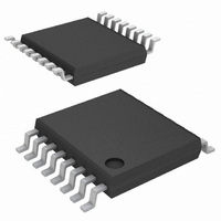
DG612AEQ-T1-E3 Vishay, DG612AEQ-T1-E3 Datasheet

DG612AEQ-T1-E3
Specifications of DG612AEQ-T1-E3
Related parts for DG612AEQ-T1-E3
DG612AEQ-T1-E3 Summary of contents
Page 1
... High-end data acquisition • Sample and hold applications • Sample and hold systems Kxx Pin 1 Device Marking: Kxx for DG611A (miniQFN16) Lxx for DG612A Pxx for DG613A xx = Date/Lot Traceability Code DG611A ON OFF Vishay Siliconix 2 pF typ.) soff - 115 maximum DG611A miniQFN ...
Page 2
... New Product GND Pxx Pin 1 Device Marking: Pxx for DG613A (miniQFN16 OFF ON Package 16-Pin TSSOP 16-Pin Narrow SOIC 16-Pin miniQFN DG613A miniQFN Top View OFF Part Number DG611AEQ-T1-E3 DG612AEQ-T1-E3 DG613AEQ-T1-E3 DG611AEY-T1-E3 DG612AEY-T1-E3 DG613AEY-T1-E3 DG611AEN-T1-E4 DG612AEN-T1-E4 DG613AEN-T1-E4 Document Number: 69904 S11-0154-Rev. B, 31-Jan-11 ...
Page 3
... New Product DG611A, DG612A, DG613A = 25 °C, unless otherwise noted) A (V (V mA, whichever occurs first c 16-Pin TSSOP d 16-Pin miniQFN e 16-Pin Narrow SOIC 16-Pin TSSOP 16-Pin miniQFN 16-Pin Narrow SOIC Vishay Siliconix Limit Unit 100 - 65 to 150 °C 450 525 mW 640 178 152 ° ...
Page 4
... DG611A, DG612A, DG613A Vishay Siliconix SPECIFICATIONS FOR DUAL SUPPLIES ( Parameter Symbol Analog Switch e V Analog Signal Range ANALOG R I On-Resistance ON R On-Resistance Match On-Resistance Flatness FLATNESS I S(off) Switch Off Leakage Current I D(off) Switch On I D(on) Leakage Current Digital Control I Input Current, V ...
Page 5
... MHz Room = 50 Room L L Room MHz Room MHz Room S D Room Full Room Full Room Full Vishay Siliconix - 40 °C to 125 ° ° ° Typ. Min. Max. Min. Max 139 180 180 235 215 120 110 ± 0.02 - 0.1 ...
Page 6
... DG611A, DG612A, DG613A Vishay Siliconix SPECIFICATIONS FOR UNIPOLAR SUPPLIES ( Parameter Symbol Analog Switch e V Analog Signal Range ANALOG R On-Resistance ON I S(off) Switch Off Leakage Current I D(off) Switch On I D(on) Leakage Current Digital Control I Input Current, V Low IN IL Input Current, V High I IH ...
Page 7
... V± = ± 6 (Dual Supply) 200 180 160 140 120 100 000 1000 100 (off 100 120 - 40 Vishay Siliconix Analog Voltage (V) COM D On-Resistance vs. V (Single Supply 125 ° ° ° ° Analog Voltage (V) COM D On-Resistance vs. Temperature (Single Supply (on) ...
Page 8
... DG611A, DG612A, DG613A Vishay Siliconix TYPICAL CHARACTERISTICS (25 °C, unless otherwise noted) 2 1nF L 2 1.5 1.0 V± = ± 0.5 0 Analog Voltage (V) Charge Injection vs. Analog Voltage 200 180 160 140 120 100 80 t OFF OFF Temperature (°C) Switching Time vs. Temperature (Single Supply) 3 ° ...
Page 9
... Switch V O Input Note: Figure 1. Switching Time 300 300 35 pF Figure 2. Break-Before-Make (DG613A Figure 3. Charge Injection Vishay Siliconix < < OFF Logic input waveform is inverted for switches that have the opposite logic sense control 3 V Logic Input Switch 0 V Output V ...
Page 10
... Bypass Figure 5. Off-Isolation Vishay Siliconix maintains worldwide manufacturing capability. Products may be manufactured at one of several qualified locations. Reliability data for Silicon Technology and Package Reliability represent a composite of all qualified locations. For related documents such as package/tape drawings, part marking, and reliability data, see www.vishay.com/ppg?69904. ...
Page 11
... Vishay product could result in personal injury or death. Customers using or selling Vishay products not expressly indicated for use in such applications their own risk and agree to fully indemnify and hold Vishay and its distributors harmless from and against any and all claims, liabilities, expenses and damages arising or resulting in connection with such use or sale, including attorneys fees, even if such claim alleges that Vishay or its distributor was negligent regarding the design or manufacture of the part ...


