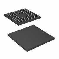
CY7C0853V-133BBC Cypress Semiconductor Corp, CY7C0853V-133BBC Datasheet - Page 7

CY7C0853V-133BBC
Manufacturer Part Number
CY7C0853V-133BBC
Description
IC,SYNC SRAM,256KX36,CMOS,BGA,172PIN,PLASTIC
Manufacturer
Cypress Semiconductor Corp
Datasheets
1.CY7C0853V-133BBC.pdf
(29 pages)
2.CY7C0853V-133BBC.pdf
(33 pages)
3.CY7C0853V-133BBC.pdf
(29 pages)
Specifications of CY7C0853V-133BBC
Format - Memory
RAM
Memory Type
SRAM - Dual Port, Synchronous
Memory Size
9M (256K x 36)
Speed
133MHz
Interface
Parallel
Voltage - Supply
3.135 V ~ 3.465 V
Operating Temperature
0°C ~ 70°C
Package / Case
172-LFBGA
Lead Free Status / RoHS Status
Contains lead / RoHS non-compliant
Available stocks
Company
Part Number
Manufacturer
Quantity
Price
Company:
Part Number:
CY7C0853V-133BBC
Manufacturer:
Cypress Semiconductor Corp
Quantity:
10 000
Part Number:
CY7C0853V-133BBC
Manufacturer:
CYPRESS/赛普拉斯
Quantity:
20 000
Document #: 38-06059 Rev. *F
Pin Definitions
A
ADS
CE0
CE1
CLK
CNTEN
CNTRST
CNT/MSK
DQ
OE
INT
CNTINT
R/W
B
MRST
TMS
TDI
TCK
TDO
V
V
0L
0L
SS
DD
0L
L
–A
–B
Left Port
L
L
L
L
L
L
–DQ
16L
3L
L
L
L
[1]
35L
L
[1]
A
ADS
CE0
CE1
CLK
CNTEN
CNTRST
CNT/MSK
DQ
OE
INT
CNTINT
R/W
B
0R
0R
Right Port
R
0R
R
–A
–B
R
R
R
R
R
–DQ
16R
3R
R
R
R
[1]
R
35R
[1]
Address Inputs.
Address Strobe Input. Used as an address qualifier. This signal should be asserted LOW
for the part using the externally supplied address on the address pins and for loading this
address into the burst address counter.
Active LOW Chip Enable Input.
Active HIGH Chip Enable Input.
Clock Signal. Maximum clock input rate is f
Counter Enable Input.
of its respective port on each rising edge of CLK. The increment is disabled if ADS or
CNTRST are asserted LOW.
Counter Reset Input.
the burst address counter of its respective port. CNTRST is not disabled by asserting ADS
or CNTEN.
Address Counter Mask Register Enable Input.
access to the mask register. When tied HIGH, the mask register is not accessible and the
address counter operations are enabled based on the status of the counter control signals.
Data Bus Input/Output.
Output Enable Input. This asynchronous signal must be asserted LOW to enable the DQ
data pins during Read operations.
Mailbox Interrupt Flag Output. The mailbox permits communications between ports. The
upper two memory locations can be used for message passing. INT
the right port writes to the mailbox location of the left port, and vice versa. An interrupt to a
port is deasserted HIGH when it reads the contents of its mailbox.
Counter Interrupt Output.
counter is incremented to all “1s.”
Read/Write Enable Input. Assert this pin LOW to write to, or HIGH to Read from the dual
port memory array.
Byte Select Inputs. Asserting these signals enables Read and Write operations to the
corresponding bytes of the memory array.
Master Reset Input. MRST is an asynchronous input signal and affects both ports. Asserting
MRST LOW performs all of the reset functions as described in the text. A MRST operation
is required at power-up.
JTAG Test Mode Select Input. It controls the advance of JTAG TAP state machine. State
machine transitions occur on the rising edge of TCK.
JTAG Test Data Input. Data on the TDI input will be shifted serially into selected registers.
JTAG Test Clock Input.
JTAG Test Data Output. TDO transitions occur on the falling edge of TCK. TDO is normally
three-stated except when captured data is shifted out of the JTAG TAP.
Ground Inputs.
Power Inputs.
PRELIMINARY
[2]
[2]
Asserting this signal LOW resets to zero the unmasked portion of
Asserting this signal LOW increments the burst address counter
[2]
CY7C0851V/CY7C0852V/CY7C0853V
This pin is asserted LOW when the unmasked portion of the
[2]
[2]
Description
MAX
.
[2]
CY7C0831V/CY7C0832V
Asserting this signal LOW enables
L
is asserted LOW when
Page 7 of 33


