CY7C0853V-133BBI Cypress Semiconductor Corp, CY7C0853V-133BBI Datasheet
CY7C0853V-133BBI
Specifications of CY7C0853V-133BBI
Available stocks


Related parts for CY7C0853V-133BBI


CY7C0853V-133BBI Summary of contents
Page 1
... North First Street • San Jose CY7C0850V/CY7C0851V CY7C0852V/CY7C0853V 4-Mbit 9-Mbit (128K x 36) (256K x 36) CY7C0852V CY7C0853V 167 133 4.0 4.7 225 270 176TQFP 172FBGA 172FBGA , CA 95134 • 408-943-2600 Revised June 24, 2004 ...
Page 2
... Document #: 38-06070 Rev. *D I/O I/O Control Control True Dual-Ported RAM Array Address Address Decode Decode TMS Reset MRST TDI JTAG Logic TCK CY7C0850V/CY7C0851V CY7C0852V/CY7C0853V 9 DQ 27R 9 DQ 18R Addr. Read Back Mask Register CNT/MSK ...
Page 3
... VDD VSS DQ25L DQ19L VSS VSS DQ19R TDI DQ7L DQ2L DQ2R DQ7R DQ5L DQ3L DQ0L DQ0R DQ3R DQ4L VDD DQ1L DQ1R VDD CY7C0850V/CY7C0851V CY7C0852V/CY7C0853V DQ13R VSS CNTINTR DQ30R DQ32R DQ14R DQ17R DQ29R DQ33R A0R INTR DQ27R DQ31R A1R NC DQ28R DQ34R DQ35R ...
Page 4
... VDD DQ26L DQ25L DQ19L VSS VSS DQ19R DQ18L TDI DQ7L DQ2L DQ2R DQ6L DQ5L DQ3L DQ0L DQ0R VSS DQ4L VDD DQ1L DQ1R CY7C0850V/CY7C0851V CY7C0852V/CY7C0853V VDD DQ13R VSS NC DQ30R DQ32R DQ14R DQ17R DQ29R DQ33R INTR DQ27R DQ31R A1R A17R DQ28R DQ34R DQ35R ...
Page 5
... A 14L [ 15L [ 16L 43 DQ 24L 44 DQ 20L Document #: 38-06070 Rev. *D 176-pin Thin Quad Flat Pack (TQFP) Top View CY7C0850V CY7C0851V CY7C0852V CY7C0850V/CY7C0851V CY7C0852V/CY7C0853V DQ 132 34R DQ 131 35R NC 130 A 129 0R A 128 1R A 127 2R A 126 3R V 125 SS V 124 ...
Page 6
... V DD Note: 3. These pins are not available for CY7C0853V device. Document #: 38-06070 Rev. *D Address Inputs. Address Strobe Input. Used as an address qualifier. This signal should be asserted LOW for the part using the externally supplied address on the address pins and for loading this address into the burst address counter ...
Page 7
... The upper two memory locations may be used for message passing and permit communications between ports. Table 2 shows the interrupt operation for both ports of CY7C0853V. The highest memory location, 3FFFF is the mailbox for the right port and 3FFFE is the mailbox for the left port. Table 2 Table 2 ...
Page 8
... The value of all three registers can be constantly maintained unchanged for an unlimited number of clock cycles. Such operation is useful in applications where wait states are needed, or when address is available a few cycles ahead of data in a shared bus interface. CY7C0850V/CY7C0851V CY7C0852V/CY7C0853V [11] An increment that results Page ...
Page 9
... Master reset (MRST) also resets the mask register to all “1s.” Document #: 38-06070 Rev. *D CY7C0850V/CY7C0851V CY7C0852V/CY7C0853V Mask Load Operation The mask register is loaded with the address value presented at the address lines. Not all values permit correct increment operations. Permitted values are of the form 2 From the most significant bit to the least significant bit, permitted values have zero or more “ ...
Page 10
... Mask 17 From Counter Figure 1. Counter, Mask, and Mirror Logic Block Diagram Document #: 38-06070 Rev. *D Load/Increment 17 Mirror Increment Logic Wrap 17 Bit CY7C0850V/CY7C0851V CY7C0852V/CY7C0853V Mask Register Counter/ Address Address Decode Register Counter To Readback 1 and Address 0 Decode 17 Wrap Wrap Detect 17 To Counter [1] RAM Array ...
Page 11
... DD . Value Reserved for version number. Defines Cypress part number for the CY7C0851V Defines Cypress part number for the CY7C0852V and CY7C0853V Defines Cypress part number for the CY7C0850V Allows unique identification of the DP family device vendor. Indicates the presence register. CY7C0850V/CY7C0851V CY7C0852V/CY7C0853V ...
Page 12
... Loads the IDR with the vendor ID code and places the register between TDI and TDO. Places BYR between TDI and TDO. Forces all CY7C0851V/CY7C0852V/ CY7C0853V output drivers to a High-Z state. Controls boundary to 1/0. Places BYR between TDI and TDO. Captures the input/output ring contents. Places BSR between TDI and TDO. ...
Page 13
... Pulse width < 20 ns. 17. C also references C OUT I/O 18 and I are not applicable for CY7C0853V because it can not be powered down by using chip enable pins. SB1 SB2 SB3 SB4 Document #: 38-06070 Rev Input Voltage .............................. –0. Output Current into Outputs (LOW)............................. 20 mA Static Discharge Voltage........................................... > 2000V (JEDEC JESD22-A114-2000B) ° ...
Page 14
... CY7C0850V/CY7C0851V CY7C0852V/CY7C0853V 3. 590 Ω 435 Ω 90% 10% < -133 -100 CY7C0853V CY7C0853V Max. Min. Max. Min. Max. 133 133 100 7.5 10.0 3.0 4.0 3.0 4.0 2.0 2.0 3.0 2.0 2.0 3.0 2.5 3 ...
Page 15
... NA 0.5 5.0 0.5 5.7 NA 5.2 6.0 6.0 7.0 7.5 7.5 6.0 6.0 6.0 6.0 7.5 7.5 6.0 6.5 5.8 7.0 -100 CY7C0853V Unit Max. Min. Max. 4.7 5 4.7 0 5.0 ns 4.7 5 1.0 ns 4.7 0 5.0 ns 4.7 1 ...
Page 16
... TCK Clock LOW to TDO Invalid TDOX JTAG Switching Waveform Test Clock TCK Test Mode Select TMS Test Data-In TDI Test Data-Out TDO Document #: 38-06070 Rev. *D Description TMSS t TMSH t TDIS t TDIH t TDOX CY7C0850V/CY7C0851V CY7C0852V/CY7C0853V 167/133/100 Min. Max. 10 100 TCYC t TDOV Page Unit MHz ...
Page 17
... Numbers are for reference only. Document #: 38-06070 Rev RSR ACTIVE t CYC2 t CL2 A A n+1 t CD2 CKLZ following the next rising edge of the clock. IH with CNT/MSK = V IL CY7C0850V/CY7C0851V CY7C0852V/CY7C0853V n+2 n n+1 t OHZ t OLZ t OE constantly loads the address on the rising edge of the CLK n+2 Page ...
Page 18
... One clock cycle is required to three-state the I/O for the Write operation on the next rising edge of CLK. Document #: 38-06070 Rev CL2 CD2 HC CD2 [25, 28, 29, 30, 31 n+1 n CD2 CKHZ Q n READ NO OPERATION CY7C0850V/CY7C0851V CY7C0852V/CY7C0853V CD2 CKHZ CKLZ CD2 CKHZ CKLZ A A n+2 n n+2 t CKLZ WRITE READ CKHZ ...
Page 19
... READ EXTERNAL ADDRESS Document #: 38-06070 Rev. *D [25, 28, 30, 31 n+1 n n+2 t CD2 OHZ READ WRITE [30] t SAD t SCN t CD2 READ WITH COUNTER CY7C0850V/CY7C0851V CY7C0852V/CY7C0853V n+3 n+4 D n+3 READ t HAD t HCN Q n+1 n+2 COUNTER HOLD READ WITH COUNTER n+5 t CD2 Q n+4 Q n+3 Page ...
Page 20
... CL2 CLK ADDRESS n INTERNAL A ADDRESS t t SAD HAD ADS CNTEN t t SCN HCN D DATA WRITE EXTERNAL ADDRESS Document #: 38-06070 Rev. *D [31 n n+1 n+1 WRITE WITH WRITE COUNTER COUNTER HOLD CY7C0850V/CY7C0851V CY7C0852V/CY7C0853V A A n+2 n n+2 n+3 WRITE WITH COUNTER A n+4 n+4 Page ...
Page 21
... RESET Notes: 32 – LOW MRST = CNT/MSK = HIGH 33. No dead cycle exists during counter reset. A Read or Write cycle may be coincidental with the counter reset. Document #: 38-06070 Rev CD2 t CKLZ WRITE READ ADDRESS 0 ADDRESS 1 ADDRESS 0 CY7C0850V/CY7C0851V CY7C0852V/CY7C0853V CD2 READ READ READ ADDRESS A ADDRESS A ...
Page 22
... the internal value of the address counter (or the mask register depending on the CNT/MSK level) being Read out on the address lines. Document #: 38-06070 Rev. *D [34, 35, 36, 37 CA2 CM2 n CD2 CKHZ CKLZ Q n INCREMENT in next clock cycle. CKLZ . CKHZ CY7C0850V/CY7C0851V CY7C0852V/CY7C0853V n+4 n+2 n n+1 n+2 n+3 Page ...
Page 23
... R_Port will Read the most recent data (written by L_Port) (t CCS Document #: 38-06070 Rev. *D [38, 39, 40 CKLZ CCS CNTRST = MRST = CNT/MSK = HIGH. 1 CY7C0850V/CY7C0851V CY7C0852V/CY7C0853V t CD2 violated, indeterminate data will be Read out. CCS + t ) after the rising edge of R_Port's clock. CYC2 CD2 + t ) after the rising edge of R_Port's clock. CYC2 CD2 Page ...
Page 24
... CNTINT goes LOW when the unmasked portion of the address counter is incremented to the maximum value. 44. The mask register assumed to have the value of 1FFFFh. 45. Retransmit happens if the counter remains in increment mode after it wraps to initially loaded value. Document #: 38-06070 Rev. *D [41, 42, 43, 44, 45] 1FFFE 1FFFD 1FFFF t SCINT CY7C0850V/CY7C0851V CY7C0852V/CY7C0853V Last_Loaded Last_Loaded +1 t RCINT Page ...
Page 25
... When CE changes state, deselection and Read happen after one cycle of latency. Document #: 38-06070 Rev n SINT 3FFFF m+1 m [1, 8, 51, 52 CNTRST = MRST = CNT/MSK = HIGH. 1 CY7C0850V/CY7C0851V CY7C0852V/CY7C0853V A A n+2 n+3 t RINT A m+3 Outputs – DQ Operation 0 35 High-Z Deselected High-Z Deselected D Write IN D Read OUT High-Z Outputs Disabled A m+4 Page ...
Page 26
... Ordering Information 256K × 36 (9M) 3.3V Synchronous CY7C0853V Dual-Port SRAM Speed (MHz) Ordering Code 133 CY7C0853V-133BBC CY7C0853V-133BBI 100 CY7C0853V-100BBC CY7C0853V-100BBI 128K × 36 (4M) 3.3V Synchronous CY7C0852V Dual-Port SRAM Speed (MHz) Ordering Code 167 CY7C0852V-167BBC CY7C0852V-167AC 133 CY7C0852V-133BBC CY7C0852V-133BBI CY7C0852V-133AC CY7C0852V-133AI 64K × 36 (2M) 3.3V Synchronous CY7C0851V Dual-Port SRAM ...
Page 27
... Package Diagrams 176-lead Thin Quad Flat Pack (24 × 24 × 1.4 mm) A176 Document #: 38-06070 Rev. *D CY7C0850V/CY7C0851V CY7C0852V/CY7C0853V 51-85132-** Page ...
Page 28
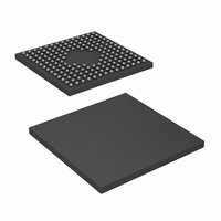
... The inclusion of Cypress products in life-support systems application implies that the manufacturer assumes all risk of such use and in doing so indemnifies Cypress against all charges. 172-Ball FBGA ( 1.25 mm) BB172 CY7C0850V/CY7C0851V CY7C0852V/CY7C0853V 51-85114-*B Page ...
Page 29
... Merged 0853 (9Mx36) with 0852 (4Mx36) and 0851(2Mx36), add 0850 (1M x36), to the datasheet. Added product selection table. Added JTAG ID code for 1M device. Added note 14. Updated boundry scan section section. Updated function description for the merge and addition. CY7C0850V/CY7C0851V CY7C0852V/CY7C0853V TM 3.3V 32K/64K/128K/256K x 36 Synchro for the CY7C0853V to 4.7 ns CKLZ Page ...