CY7C0853V-133BBC Cypress Semiconductor Corp, CY7C0853V-133BBC Datasheet
CY7C0853V-133BBC
Manufacturer Part Number
CY7C0853V-133BBC
Description
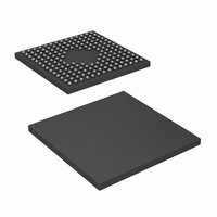
IC,SYNC SRAM,256KX36,CMOS,BGA,172PIN,PLASTIC
Manufacturer
Cypress Semiconductor Corp
Datasheets
1.CY7C0853V-133BBC.pdf
(29 pages)
2.CY7C0853V-133BBC.pdf
(33 pages)
3.CY7C0853V-133BBC.pdf
(29 pages)
Specifications of CY7C0853V-133BBC
Format - Memory
RAM
Memory Type
SRAM - Dual Port, Synchronous
Memory Size
9M (256K x 36)
Speed
133MHz
Interface
Parallel
Voltage - Supply
3.135 V ~ 3.465 V
Operating Temperature
0°C ~ 70°C
Package / Case
172-LFBGA
Lead Free Status / RoHS Status
Contains lead / RoHS non-compliant
Available stocks
Company
Part Number
Manufacturer
Quantity
Price
Company:

Part Number:
CY7C0853V-133BBC
Manufacturer:
Cypress Semiconductor Corp
Quantity:
10 000
Part Number:
CY7C0853V-133BBC
Manufacturer:
CYPRESS/赛普拉斯
Quantity:
20 000


Cypress Semiconductor Corporation
Document #: 38-06059 Rev. *F
Features (all)
Features (all except CY7C0853V)
• True dual-ported memory cells that allow simultaneous
• Synchronous pipelined
• Organization of 2M, 4.5M, and 9M devices
• Pipelined output mode allows fast 167-MHz operation
• 0.18-micron CMOS for optimum speed and power
• High-speed clock to data access: 4.0 ns (max.)
• 3.3V low operating power
• Interrupt flags for message passing
• Global master reset
• Separate byte enables on both ports
• Commercial and industrial temperature ranges
• IEEE 1149.1-compatible JTAG boundary scan
• 172-ball BGA (1 mm pitch) (15 mm × 15 mm)
• 120-pin TQFP (14 mm × 14 mm × 1.4 mm)
• 176-pin TQFP (24 mm × 24 mm × 1.4 mm)
• FLEx36
• Counter wrap around control
• Counter readback on address lines
• Mask register readback on address lines
• Dual Chip Enables on both ports for easy depth
access of the same memory location
2M to 4M to 9M
expansion
— 256K × 36 (CY7C0853V)
— 128K × 36 (CY7C0852V)
— 64K × 36 (CY7C0851V)
— 256K × 18 (CY7C0832V)
— 128K × 18 (CY7C0831V)
— Active = 300 mA (typical)
— Standby = 10 mA (typical)
— Internal mask register controls counter wrap-around
— Counter-interrupt flags to indicate wrap-around
— Memory block retransmit operation
devices are pin footprint upgradeable from
3.3V 64K/128K/256K x 36 and 128K/256K x 18
•
3901 North First Street
PRELIMINARY
Functional Description (all)
The CY7C085XV/CY7C083XV are 2M, 4.5M, and 9M
pipelined, synchronous, true dual-port static RAMs that are
high-speed, low-power 3.3V CMOS. Two ports are provided,
permitting independent, simultaneous access for Reads from
any location in memory. A particular port can write to a certain
location while another port is reading that location. The result
of writing to the same location by more than one port at the
same time is undefined. Registers on control, address, and
data lines allow for minimal set-up and hold time.
Functional Description (all except CY7C0853V)
During a Read operation, data is registered for decreased
cycle time. Clock to data valid t
port contains a burst counter on the input address register.
After externally loading the counter with the initial address, the
counter will increment the address internally (more details to
follow). The internal Write pulse width is independent of the
duration of the R/W input signal. The internal Write pulse is
self-timed to allow the shortest possible cycle times.
A HIGH on CE0 or LOW on CE1 for one clock cycle will power
down the internal circuitry to reduce the static power
consumption. One cycle with chip enables asserted is required
to reactivate the outputs.
Counter enable (CNTEN) inputs are provided to stall the
operation of the address input and utilize the internal address
generated by the internal counter for fast, interleaved memory
applications. A port’s burst counter is loaded when the port’s
address strobe (ADS) and CNTEN signals are LOW. When the
port’s CNTEN is asserted and the ADS is deasserted, the
address counter will increment on each LOW to HIGH
transition of that port’s clock signal. This will Read/Write one
word from/into each successive address location until CNTEN
is deasserted. The counter can address the entire memory
array, and will loop back to the start. Counter reset (CNTRST)
is used to reset the unmasked portion of the burst counter to
0s. A counter-mask register is used to control the counter
wrap. The counter and mask register operations are described
in more detail in the following sections.
New features added to the CY7C08X1V/CY7C08X2V devices
include: readback of burst-counter internal address value on
address lines, counter-mask registers to control the counter
wrap-around, counter interrupt (CNTINT) flags, readback of
mask register value on address lines, retransmit functionality,
interrupt flags for message passing, JTAG for boundary scan,
and asynchronous Master Reset (MRST).
CY7C0851V/CY7C0852V/CY7C0853V
Synchronous Dual-Port RAM
•
San Jose
CY7C0831V/CY7C0832V
,
CA 95134
CD2
Revised January 22, 2003
= 4.0 ns at 167 MHz. Each
•
408-943-2600
Related parts for CY7C0853V-133BBC
Image
Part Number
Description
Manufacturer
Datasheet
Request
R

Part Number:
Description:
CY7C0853V-133BBXI
Manufacturer:
Cypress Semiconductor Corp
Datasheet:
Part Number:
Description:
IC,SYNC SRAM,256KX36,CMOS,BGA,172PIN,PLASTIC
Manufacturer:
Cypress Semiconductor Corp
Datasheet:
Part Number:
Description:
IC,SYNC SRAM,256KX36,CMOS,BGA,172PIN,PLASTIC
Manufacturer:
Cypress Semiconductor Corp
Datasheet:

Part Number:
Description:
Manufacturer:
Cypress Semiconductor Corp
Datasheet:
Part Number:
Description:
Manufacturer:
Cypress Semiconductor Corp
Datasheet:
Part Number:
Description:
Manufacturer:
Cypress Semiconductor Corp
Datasheet:
Part Number:
Description:
Manufacturer:
Cypress Semiconductor Corp
Datasheet: