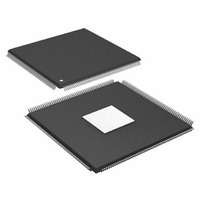
ADSP-21369BSWZ-2A Analog Devices Inc, ADSP-21369BSWZ-2A Datasheet - Page 17

ADSP-21369BSWZ-2A
Manufacturer Part Number
ADSP-21369BSWZ-2A
Description
333 MHz, Shared Memory,S/PDIF EPAD PBfr
Manufacturer
Analog Devices Inc
Series
SHARC®r
Type
Floating Pointr
Datasheet
1.ADSP-21369KBPZ-2A.pdf
(60 pages)
Specifications of ADSP-21369BSWZ-2A
Interface
DAI, DPI
Clock Rate
333MHz
Non-volatile Memory
ROM (768 kB)
On-chip Ram
256kB
Voltage - I/o
3.30V
Voltage - Core
1.20V
Operating Temperature
-40°C ~ 85°C
Mounting Type
Surface Mount
Package / Case
208-LQFP
Device Core Size
32/40Bit
Architecture
Super Harvard
Format
Floating Point
Clock Freq (max)
333MHz
Mips
333
Device Input Clock Speed
333MHz
Ram Size
256KB
Program Memory Size
768KB
Operating Supply Voltage (typ)
1.2/3.3V
Operating Supply Voltage (min)
1.14/3.13V
Operating Supply Voltage (max)
1.26/3.47V
Operating Temp Range
-40C to 85C
Operating Temperature Classification
Industrial
Mounting
Surface Mount
Pin Count
208
Package Type
LQFP EP
Package
208LQFP EP
Numeric And Arithmetic Format
Floating-Point
Maximum Speed
333 MHz
Device Million Instructions Per Second
333 MIPS
Lead Free Status / RoHS Status
Lead free / RoHS Compliant
Lead Free Status / RoHS Status
Lead free / RoHS Compliant
Available stocks
Company
Part Number
Manufacturer
Quantity
Price
Company:
Part Number:
ADSP-21369BSWZ-2A
Manufacturer:
Analog Devices Inc
Quantity:
10 000
ELECTRICAL CHARACTERISTICS
1
2
3
4
5
6
7
8
9
10
11
12
13
Applies to output and bidirectional pins: ADDRx, DATAx, RD, WR, MSx, BRx, FLAGx, DAI_Px, DPI_Px, SDRAS, SDCAS, SDWE, SDCKE, SDA10, SDCLKx, EMU, TDO.
See
Applies to input pins without internal pull-ups: BOOT_CFGx, CLK_CFGx, CLKIN, RESET, TCK.
Applies to input pins with internal pull-ups: ACK, RPBA, TMS, TDI, TRST.
Applies to input pins with internal pull-downs: IDx.
Applies to input pins with internal pull-ups disabled: ACK, RPBA.
Applies to three-statable pins without internal pull-ups: FLAGx, SDCLKx, TDO.
Applies to three-statable pins with internal pull-ups: ADDRx, DATAx, RD, WR, MSx, BRx, DAI_Px, DPI_Px, SDRAS, SDCAS, SDWE, SDCKE, SDA10, EMU.
Applies to three-statable pins with internal pull-ups disabled: ADDRx, DATAx, RD, WR, MSx, BRx, DAI_Px, DPI_Px, SDRAS, SDCAS, SDWE, SDCKE, SDA10
See Estimating Power Dissipation for ADSP-21368 SHARC Processors (EE-299) for further information.
Characterized, but not tested.
Applies to all signal pins.
Guaranteed, but not tested.
Parameter
V
V
I
I
I
I
I
I
I
I
AI
C
IH
IL
IHPD
ILPU
OZH
OZL
OZLPU
DD
OH
OL
3, 5, 6
IN
3, 4
-
DD
7, 9
12, 13
Output Drive Currents on Page 48
1
INTYP
4
1
5
7, 8
11
8
10
Description
High Level Output Voltage
Low Level Output Voltage
High Level Input Current
Low Level Input Current
High Level Input Current Pull-Down
Low Level Input Current Pull-Up
Three-State Leakage Current
Three-State Leakage Current
Three-State Leakage Current Pull-Up
Supply Current (Internal)
Supply Current (Analog)
Input Capacitance
for typical drive current capabilities.
Rev. E | Page 17 of 60 | July 2009
Test Conditions
@ V
@ V
@ V
@ V
@ V
@ V
@ V
@ V
@ V
t
t
t
t
t
A
f
IN
CCLK
CCLK
CCLK
CCLK
CCLK
VDD
= 1 MHz, T
DDEXT
DDEXT
DDEXT
DDEXT
DDEXT
DDEXT
DDEXT
DDEXT
DDEXT
= 3.75 ns, V
= 3.00 ns, V
= 2.85 ns, V
= 2.73 ns, V
= 2.50 ns, V
= Max
= Min, I
= Min, I
= Max, V
= Max, V
= Max, V
= Max, V
= Max, V
= Max, V
= Max, V
ADSP-21367/ADSP-21368/ADSP-21369
CASE
OH
OL
DDINT
DDINT
DDINT
DDINT
DDINT
= 25°C, V
IN
IN
IN
IN
IN
IN
IN
= 1.0 mA
= –1.0 mA
= V
= 0 V
= 0 V
= 0 V
= V
= 0 V
= 0 V
= 1.2 V, 25°C
= 1.2 V, 25°C
= 1.3 V, 25°C
= 1.3 V, 25°C
= 1.3 V, 25°C
DDEXT
DDEXT
Max
Max
IN
2
= 1.3 V
2
Min
2.4
Typ
700
900
1050
1080
1100
Max
0.4
10
10
250
200
10
10
200
11
4.7
Unit
V
V
μA
μA
μA
μA
μA
μA
μA
mA
mA
mA
mA
mA
mA
pF


