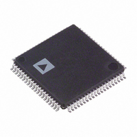
AD9985KSTZ-140 Analog Devices Inc, AD9985KSTZ-140 Datasheet - Page 27

AD9985KSTZ-140
Manufacturer Part Number
AD9985KSTZ-140
Description
IC,Data Acquisition Signal Conditioner,3-CHANNEL,8-BIT,CMOS,QFP,80PIN,PLASTIC
Manufacturer
Analog Devices Inc
Datasheet
1.AD9985KSTZ-110.pdf
(32 pages)
Specifications of AD9985KSTZ-140
Applications
Video
Interface
Serial Port
Voltage - Supply
2.2 V ~ 3.45 V
Package / Case
80-LQFP
Mounting Type
Surface Mount
Lead Free Status / RoHS Status
Lead free / RoHS Compliant
Available stocks
Company
Part Number
Manufacturer
Quantity
Price
Company:
Part Number:
AD9985KSTZ-140
Manufacturer:
ADI
Quantity:
717
Company:
Part Number:
AD9985KSTZ-140
Manufacturer:
Analog Devices Inc
Quantity:
10 000
Part Number:
AD9985KSTZ-140
Manufacturer:
ADI/亚德诺
Quantity:
20 000
Data is read from the control registers of the AD9985 in a
similar manner. Reading requires two data transfer operations:
The base address must be written with the R/W bit of the slave
address byte low to set up a sequential read operation.
Reading (the R/ W bit of the slave address byte high) begins at
the previously established base address. The address of the read
register autoincrements after each byte is transferred.
To terminate a read/write sequence to the AD9985, a stop signal
must be sent. A stop signal comprises a low-to-high transition
of SDA while SCL is high.
A repeated start signal occurs when the master device driving
the serial interface generates a start signal without first
generating a stop signal to terminate the current communi-
cation. This is used to change the mode of communication
(read, write) between the slave and master without releasing the
serial interface lines.
Serial Interface Read/Write Examples
Write to one control register
•
•
•
•
•
Write to four consecutive control registers
•
•
•
Start Signal
Slave Address Byte (R/ W Bit = Low)
Base Address Byte
Data Byte to Base Address
Stop Signal
Start Signal
Slave Address Byte (R/ W Bit = Low)
Base Address Byte
Rev. 0 | Page 27 of 32
•
•
•
•
•
Read from one control register
•
•
•
•
•
•
•
Read from four consecutive control registers
•
•
•
•
•
•
•
•
•
•
SCL
SDA
Data Byte to Base Address
Data Byte to (Base Address + 1)
Data Byte to (Base Address + 2)
Data Byte to (Base Address + 3)
Stop Signal
Start Signal
Slave Address Byte (R/ W Bit = Low)
Base Address Byte
Start Signal
Slave Address Byte (R/ W Bit = High)
Data Byte from Base Address
Stop Signal
Start Signal
Slave Address Byte (R/ W Bit = Low)
Base Address Byte
Start Signal
Slave Address Byte (R/ W Bit = High)
Data Byte from Base Address
Data Byte from (Base Address + 1)
Data Byte from (Base Address + 2)
Data Byte from (Base Address + 3)
Stop Signal
BIT 7
Figure 13. Serial Interface—Typical Byte Transfer
BIT 6
BIT 5
BIT 4
BIT 3
BIT 2
BIT 1
BIT 0
AD9985
ACK


