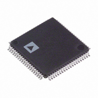
AD9985KSTZ-140 Analog Devices Inc, AD9985KSTZ-140 Datasheet - Page 12

AD9985KSTZ-140
Manufacturer Part Number
AD9985KSTZ-140
Description
IC,Data Acquisition Signal Conditioner,3-CHANNEL,8-BIT,CMOS,QFP,80PIN,PLASTIC
Manufacturer
Analog Devices Inc
Datasheet
1.AD9985KSTZ-110.pdf
(32 pages)
Specifications of AD9985KSTZ-140
Applications
Video
Interface
Serial Port
Voltage - Supply
2.2 V ~ 3.45 V
Package / Case
80-LQFP
Mounting Type
Surface Mount
Lead Free Status / RoHS Status
Lead free / RoHS Compliant
Available stocks
Company
Part Number
Manufacturer
Quantity
Price
Company:
Part Number:
AD9985KSTZ-140
Manufacturer:
ADI
Quantity:
717
Company:
Part Number:
AD9985KSTZ-140
Manufacturer:
Analog Devices Inc
Quantity:
10 000
Part Number:
AD9985KSTZ-140
Manufacturer:
ADI/亚德诺
Quantity:
20 000
AD9985
input is present. The offset then remains in place when other
signal levels are processed, and the entire signal is shifted to
eliminate offset errors.
In most PC graphics systems, black is transmitted between
active video lines. With CRT displays, when the electron beam
has completed writing a horizontal line on the screen (at the
right side), the beam is deflected quickly to the left side of the
screen (called horizontal retrace), and a black signal is provided
to prevent the beam from disturbing the image.
In systems with embedded sync, a blacker-than-black signal
(Hsync) is produced briefly to signal the CRT that it is time to
begin a retrace. For obvious reasons, it is important to avoid
clamping on the tip of Hsync. Fortunately, there is virtually
always a period following Hsync, called the back porch, where a
good black reference is provided. This is the time when
clamping should be done.
The clamp timing can be established by simply exercising the
CLAMP pin at the appropriate time (with External Clamp = 1).
The polarity of this signal is set by the clamp polarity bit.
A simpler method of clamp timing employs the AD9985
internal clamp timing generator. The clamp placement register
is programmed with the number of pixel times that should pass
after the trailing edge of HSYNC before clamping starts. A
second register (clamp duration) sets the duration of the clamp.
These are both 8-bit values, providing considerable flexibility in
clamp generation. The clamp timing is referenced to the trailing
edge of Hsync because, though Hsync duration can vary widely,
the back porch (black reference) always follows Hsync. A good
starting point for establishing clamping is to set the clamp
placement to 09H (providing 9 pixel periods for the graphics
signal to stabilize after sync) and set the clamp duration to 14H
(giving the clamp 20 pixel periods to reestablish the black
reference).
Clamping is accomplished by placing an appropriate charge on
the external input coupling capacitor. The value of this capacitor
affects the performance of the clamp. If it is too small, there will
be a significant amplitude change during a horizontal line time
(between clamping intervals). If the capacitor is too large, then
it will take excessively long for the clamp to recover from a large
change in incoming signal offset. The recommended value
(47 nF) results in recovering from a step error of 100 mV to
within 1/2 LSB in 10 lines with a clamp duration of 20 pixel
periods on a 60 Hz SXGA signal.
YUV Clamping
YUV graphic signals are slightly different from RGB signals in
that the dc reference level (black level in RGB signals) can be at
the midpoint of the graphics signal rather than at the bottom.
For these signals, it can be necessary to clamp to the midscale
range of the A/D converter range (80H) rather than at the
bottom of the A/D converter range (00H).
Rev. 0 | Page 12 of 32
Clamping to midscale rather than to ground can be accom-
plished by setting the clamp select bits in the serial bus register.
Each of the three converters has its own selection bit so that
they can be clamped to either midscale or ground inde-
pendently. These bits are located in Register 10H and are
Bits 0–2. The midscale reference voltage that each A/D
converter clamps to is provided on the MIDSCV pin (Pin 37).
This pin should be bypassed to ground with a 0.1 µF capacitor,
even if midscale clamping is not required.
GAIN AND OFFSET CONTROL
The AD9985 can accommodate input signals with inputs
ranging from 0.5 V to 1.0 V full scale. The full-scale range is set
in three 8-bit registers (Red Gain, Green Gain, and Blue Gain).
Note that increasing the gain setting results in an image with less
contrast.
The offset control shifts the entire input range, resulting in a
change in image brightness. Three 7-bit registers (Red Offset,
Green Offset, Blue Offset) provide independent settings for
each channel. The offset controls provide a ±63 LSB adjustment
range. This range is connected with the full-scale range, so if the
input range is doubled (from 0.5 V to 1.0 V) then the offset step
size is also doubled (from 2 mV per step to 4 mV per step).
Figure 4 illustrates the interaction of gain and offset controls.
The magnitude of an LSB in offset adjustment is proportional to
the full-scale range, so changing the full-scale range also
changes the offset. The change is minimal if the offset setting is
near midscale. When changing the offset, the full-scale range is
not affected, but the full-scale level is shifted by the same
amount as the zero-scale level.
Auto Offset
In addition to the manual offset adjustment mode (via
Registers 0Bh to 0Dh), the AD9985 also includes circuitry to
automatically calibrate the offset for each channel. By
monitoring the output of each ADC during the back porch of
the input signals, the AD9985 can self-adjust to eliminate any
1.0
0.5
0
00H
Figure 4. Gain and Offset Control
GAIN
OFFSET = 7FH
OFFSET = 3FH
OFFSET = 00H
OFFSET = 7FH
OFFSET = 3FH
OFFSET = 00H
FFH


