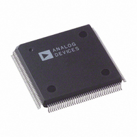
AD9887AKSZ-140 Analog Devices Inc, AD9887AKSZ-140 Datasheet - Page 43

AD9887AKSZ-140
Manufacturer Part Number
AD9887AKSZ-140
Description
IC,TV/VIDEO CIRCUIT,Video Digitizer,CMOS,QFP,160PIN,PLASTIC
Manufacturer
Analog Devices Inc
Datasheet
1.AD9887AKSZ-140.pdf
(52 pages)
Specifications of AD9887AKSZ-140
Applications
Graphic Cards, VGA Interfaces
Interface
Analog and Digital
Voltage - Supply
3.15 V ~ 3.45 V
Package / Case
160-MQFP, 160-PQFP
Mounting Type
Surface Mount
Lead Free Status / RoHS Status
Lead free / RoHS Compliant
Available stocks
Company
Part Number
Manufacturer
Quantity
Price
Company:
Part Number:
AD9887AKSZ-140
Manufacturer:
MAX
Quantity:
59
Company:
Part Number:
AD9887AKSZ-140
Manufacturer:
ADI
Quantity:
364
Company:
Part Number:
AD9887AKSZ-140
Manufacturer:
Analog Devices Inc
Quantity:
10 000
Part Number:
AD9887AKSZ-140
Manufacturer:
ADI/亚德诺
Quantity:
20 000
0x17 7:0
0x18 7:0
0x19 7:0
0x1A 7:0
0x1B 7:0
0x1C 7:3
0x1C 2
Table 51. 4:2:2 Input/Output Configuration
Channel
Red
Green
Blue
0x1C 1
This register allows the coast signal to be applied prior to
the Vsync signal. This is necessary in cases where pre-
equalization pulses are present. This register defines the
number of edges that are filtered before Vsync on a
composite sync.
The default is 0.
This register allows the coast signal to be applied
following the Vsync signal. This is necessary when
postequalization pulses are present. This register defines
the number of edges that are filtered after Vsync on a
composite sync.
The default is 0.
Must be set to 0x41 for proper operation.
Must be set to 00000*** for autogain mode and 00101***
for manual-gain mode.
In 4:2:2 mode, the red and blue channels can be
interchanged to help satisfy board layout or timing
requirements, but the green channel must be configured
for Y. Register 0x1C, Bit 2, controls the order that the
U/V (CbCr) data is output. If this bit is high, the red
channel data precedes the blue channel data. If this bit is
low, the blue channel data precedes the red channel data.
See the example in Table 51.
Must be set to 0 for standard input sampling.
Must be set to default.
Must be set to 0x00 for autogain mode and 0x10 for
manual-gain mode.
Input
Connection
Y
Y
U
Precoast
Postcoast
Test
Test
Test
Test
CbCr Output Order
Test Bits
Output Format
V/U if 0x1C Bit 2 = 1;
U/V if 0x1C Bit 2 = 0
Y
High impedance
Rev. B | Page 43 of 52
0x1C 0
Table 52. 4:2:2 Output Mode Select
Select
1
0
0x1D 6
Table 53. HDCP Key Status
Select
1
0
0x1E 7:0
0x1F 7:0
0x20 7
Table 54. HDCP A0 Serial Address
Select
1
0
0x20 6
Table 55. MDA Pin Select
Select
1
0
0x20 5
Table 56. Analog Input Bandwidth Control
Select
0
1
4:2:2 mode can be used to reduce the number of data
lines used from 24 to 16 for applications using YUV,
YCbCr, or YPbPr graphics signals. See Figure 27 for a
timing diagram for this mode.
This bit indicates the presence of HDCP keys read from
the external EEPROM.
Must be set to 0xFF for proper operation.
Must be set to 0x84 for proper operation.
This bit sets the value of the A0 bit for the DDC
serial port.
The default setting is 0.
This bit sets the function of Pin 49 to MDA when set at 1.
The default setting is 0.
This bit controls the analog input bandwidth.
The default setting 0.
4:2:2 Output Mode Select
HDCP Keys Detected
Test Register
Test Register
Analog Input Bandwidth Control
HDCP A0 Serial Address Bit
MDA Pin Select
Output Mode
4:4:4
4:2:2
HDCP Key Status
HDCP keys present
HDCP keys not present
Serial Address
A0 bit = 1, address = 0x76
A0 bit = 0, address = 0x74
Output Mode
Pin 49 = MDA for HDCP
Pin 49 = CTL3 signal
Input Bandwidth
High analog input bandwidth
Low analog input bandwidth
AD9887A


