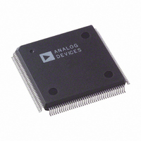
AD9887AKSZ-140 Analog Devices Inc, AD9887AKSZ-140 Datasheet - Page 39

AD9887AKSZ-140
Manufacturer Part Number
AD9887AKSZ-140
Description
IC,TV/VIDEO CIRCUIT,Video Digitizer,CMOS,QFP,160PIN,PLASTIC
Manufacturer
Analog Devices Inc
Datasheet
1.AD9887AKSZ-140.pdf
(52 pages)
Specifications of AD9887AKSZ-140
Applications
Graphic Cards, VGA Interfaces
Interface
Analog and Digital
Voltage - Supply
3.15 V ~ 3.45 V
Package / Case
160-MQFP, 160-PQFP
Mounting Type
Surface Mount
Lead Free Status / RoHS Status
Lead free / RoHS Compliant
Available stocks
Company
Part Number
Manufacturer
Quantity
Price
Company:
Part Number:
AD9887AKSZ-140
Manufacturer:
MAX
Quantity:
59
Company:
Part Number:
AD9887AKSZ-140
Manufacturer:
ADI
Quantity:
364
Company:
Part Number:
AD9887AKSZ-140
Manufacturer:
Analog Devices Inc
Quantity:
10 000
Part Number:
AD9887AKSZ-140
Manufacturer:
ADI/亚德诺
Quantity:
20 000
0x0F 1
Table 23. Green Clamp Select Settings
Clamp
0
1
0x0F 0
Table 24. Blue Clamp Select Settings
Clamp
0
1
Mode Control 2
0x10 7
Table 25. Data Output Clock Invert (CKINV) Settings
CKINV
0
1
0x10 6
Table 26. Pixel Select Settings
Pixel Select
0
1
A bit that determines whether the green channel is
clamped to ground or to midscale.
A bit that determines whether the blue channel is
clamped to ground or to midscale.
A control bit for the inversion of the output data clocks
(Pin 134 and Pin 135). This function only works for the
digital interface. When not inverted, data is output upon
the trailing edge of the data clock. See Figure 37 through
Figure 40 for how this affects timing.
This bit selects either one or two pixels per clock mode
for the digital interface. It determines whether the
output is from a single port (even port only) at the full
data rate, or from two ports (both even and odd ports) at
half the full data rate per port. Logic 0 selects one pixel
per clock (even port only). Logic 1 selects two pixels per
clock (both ports). See the Digital Interface Timing
Diagrams (Figure 37 through Figure 40) for visual
representations of this function. Note that this function
operates exactly like the demux function on the analog
interface.
The default setting for this register is 0.
The default for this register is 0.
The default for this register is 0.
The default setting for this register is 0.
Green Clamp Select
Blue Clamp Select
Data Output Clock Invert (CKINV)
Pixel Select
Function
Clamp to ground
Clamp to midscale (Pin 109)
Function
Clamp to ground
Clamp to midscale (Pin 99)
One pixel per clock
Two pixels per clock
Function
Function
Not inverted
Inverted
Rev. B | Page 39 of 52
0x10 5, 4
Table 27. Output Drive Strength Settings
Bit 5
1
0
0
0x10 3
Table 28. Power-Down Output (PDO) Settings
PDO
0
1
0x10 2
Table 29. Sync Detect Polarity Settings
Polarity
0
1
These two bits select the drive strength for the high
speed digital outputs (all data output and clock output
pins). Higher drive strength results in faster rise/fall
times and enables easier capture of data in general.
Lower drive strength results in slower rise/fall times and
reduces EMI and digitally generated power supply noise.
The exact timing specifications for each of these modes
are specified in Table 7.
This bit can put the outputs into a high impedance mode.
This applies to all outputs except SOGOUT and REFOUT.
This pin controls the polarity of the sync detect output
pin (Pin 136).
The default for this register is 11. This option works on
both the analog and digital interfaces.
The default for this register is 0. This option works on
both the analog and digital interfaces.
The default for this register is 0. This option works on
both the analog and digital interfaces.
Bit 4
X
1
0
Output Drive
Sync Detect Polarity
Power-Down Outputs (PDO)
Function
Activity = Logic 1 output
Activity = Logic 0 output
Function
Normal operation
Three-state
Result
High drive strength
Medium drive strength
Low drive strength
AD9887A


