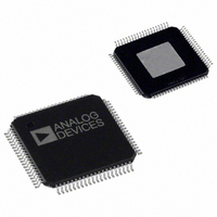
AD9775BSVZ Analog Devices Inc, AD9775BSVZ Datasheet - Page 27

AD9775BSVZ
Manufacturer Part Number
AD9775BSVZ
Description
IC,D/A CONVERTER,DUAL,14-BIT,CMOS,TQFP,80PIN
Manufacturer
Analog Devices Inc
Series
TxDAC+®r
Datasheet
1.AD9775BSVZRL.pdf
(56 pages)
Specifications of AD9775BSVZ
Settling Time
11ns
Number Of Bits
14
Data Interface
Parallel
Number Of Converters
2
Voltage Supply Source
Analog and Digital
Power Dissipation (max)
410mW
Operating Temperature
-40°C ~ 85°C
Mounting Type
Surface Mount
Package / Case
80-TQFP Exposed Pad, 80-eTQFP, 80-HTQFP, 80-VQFP
Number Of Channels
2
Resolution
14b
Interface Type
Parallel
Single Supply Voltage (typ)
3.3V
Dual Supply Voltage (typ)
Not RequiredV
Architecture
R-2R
Power Supply Requirement
Analog and Digital
Output Type
Current
Single Supply Voltage (min)
3.1V
Single Supply Voltage (max)
3.5V
Dual Supply Voltage (min)
Not RequiredV
Dual Supply Voltage (max)
Not RequiredV
Operating Temp Range
-40C to 85C
Operating Temperature Classification
Industrial
Mounting
Surface Mount
Pin Count
80
Lead Free Status / RoHS Status
Lead free / RoHS Compliant
For Use With
AD9775-EBZ - BOARD EVALUATION FOR AD9775
Lead Free Status / Rohs Status
Compliant
Available stocks
Company
Part Number
Manufacturer
Quantity
Price
Company:
Part Number:
AD9775BSVZ
Manufacturer:
Analog Devices Inc
Quantity:
135
Company:
Part Number:
AD9775BSVZ
Manufacturer:
Analog Devices Inc
Quantity:
10 000
Part Number:
AD9775BSVZ
Manufacturer:
ADI/亚德诺
Quantity:
20 000
Company:
Part Number:
AD9775BSVZRL
Manufacturer:
Analog Devices Inc
Quantity:
10 000
In addition, if the zero-stuffing option is enabled, the VCO
doubles its speed again. Phase noise may be slightly higher with
the PLL enabled. Figure 47 illustrates typical phase noise perform-
ance of the AD9775 with 2× interpolation and various input
data rates. The signal synthesized for the phase noise measurement
was a single carrier at a frequency of f
nature of this signal eliminates quantization noise and distortion
spurs as a factor in the measurement. Although the curves blend
together in Figure 47, the different conditions are given for clarity
in Table 19. Figure 47 also contains a table detailing the maximum
and minimum f
rate and PLL divider setting. These rates are guaranteed over
the entire supply and operating temperature range. Figure 48
shows typical performance of the PLL lock signal (Pin 8 or
Pin 53) when the PLL is in the process of locking.
Table 19. Required PLL Prescaler Ratio vs. f
f
125 MSPS
125 MSPS
100 MSPS
75 MSPS
50 MSPS
DATA
–100
–110
Figure 48. PLL_LOCK Output Signal (Pin 8) in the Process of Locking
–10
–20
–30
–40
–50
–60
–70
–80
–90
0
0
DATA
1
Figure 47. Phase Noise Performance
PLL
Disabled
Enabled
Enabled
Enabled
Enabled
rates for each combination of interpolation
FREQUENCY OFFSET (MHz)
(Typical Lock Time)
2
Prescaler Ratio
Div 1
Div 2
Div 2
Div 4
3
DATA
/4. The repetitive
4
DATA
5
Rev. E | Page 27 of 56
It is important to note that the resistor/capacitor needed for the
PLL loop filter is internal on the AD9775. This suffices unless the
input data rate is below 10 MHz, in which case an external series
RC is required between the LPF pin and CLKVDD pins.
POWER DISSIPATION
The AD9775 has three voltage supplies: DVDD, AVDD, and
CLKVDD. Figure 49 through Figure 51 show the current
required from each of these supplies when each is set to the 3.3 V
nominal specified for the AD9775. Power dissipation (P
easily be extracted by multiplying the given curves by 3.3. As
Figure 49 shows, I
the interpolation rate, and the activation of the internal digital
modulator. I
modulation rate by itself. In Figure 50, I
of sensitivity to the data, the interpolation rate, and the modu-
lator function but to a much lesser degree (<10%). In Figure 51,
I
percentage of the overall AD9775 supply current requirements.
CLKVDD
76.0
75.5
75.0
74.5
74.0
73.5
73.0
72.5
72.0
400
350
300
250
200
150
100
50
0
varies over a wide range yet is responsible for only a small
0
0
Figure 49. I
Figure 50. I
8 × , (MOD. ON)
DVDD
8 × , (MOD. ON)
, however, is relatively insensitive to the
DVDD
AVDD
8 ×
8 ×
DVDD
50
50
vs. f
vs. f
is very dependent on the input data rate,
DATA
DATA
4 ×
4 ×
vs. Interpolation Rate, PLL Disabled
vs. Interpolation Rate, PLL Disabled
f
f
DATA
DATA
4 × , (MOD. ON)
100
100
(MHz)
(MHz)
4 × , (MOD. ON)
AVDD
2 × , (MOD. ON)
150
150
2 × , (MOD. ON)
shows the same type
1 ×
1 ×
2 ×
2 ×
AD9775
200
200
D
) can


