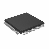
AD8197AASTZ-RL Analog Devices Inc, AD8197AASTZ-RL Datasheet - Page 14

AD8197AASTZ-RL
Manufacturer Part Number
AD8197AASTZ-RL
Description
IC,Telecom Switching Circuit,QFP,100PIN,PLASTIC
Manufacturer
Analog Devices Inc
Datasheet
1.AD8197AASTZ-RL.pdf
(28 pages)
Specifications of AD8197AASTZ-RL
Function
Switch
Circuit
1 x 4:1
On-state Resistance
50 Ohm
Voltage Supply Source
Single Supply
Voltage - Supply, Single/dual (±)
3 V ~ 3.6 V
Current - Supply
40mA
Operating Temperature
-40°C ~ 85°C
Mounting Type
Surface Mount
Package / Case
100-LQFP
Lead Free Status / RoHS Status
Lead free / RoHS Compliant
Available stocks
Company
Part Number
Manufacturer
Quantity
Price
Company:
Part Number:
AD8197AASTZ-RL
Manufacturer:
Analog Devices Inc
Quantity:
10 000
AD8197A
The AD8197A requires output termination resistors when the
high speed outputs are enabled. Termination can be internal
and/or external. The internal terminations of the AD8197A are
enabled by programming the TX_PTO bit of the transmitter
settings register or by setting the PP_OTO pin of the parallel
control interface. The internal terminations of the AD8197A
default to the setting indicated by PP_OTO upon reset. External
terminations can be provided either by on-board resistors or by
the input termination resistors of an HDMI/DVI receiver. If
both the internal terminations are enabled and external termi-
nations are present, set the output current level to 20 mA by
programming the TX_OCL bit of the transmitter settings
register through the serial control interface or by setting the
PP_OCL pin of the parallel control interface. The output
current level defaults to the level indicated by PP_OCL upon
reset. If only external terminations are provided (if the internal
terminations are disabled), set the output current level to 10 mA
by programming the TX_OCL bit of the transmitter settings
register or by setting the PP_OCL pin of the parallel control
interface. The high speed outputs must be disabled if there are
no output termination resistors present in the system.
The output pre-emphasis can be manually configured to provide
one of four different levels of high frequency boost. The specific
boost level is selected by programming the TX_PE bits of the
transmitter settings register through the serial control interface,
or by setting the PP_PE bus of the parallel control interface. No
specific cable length is suggested for a particular pre-emphasis
setting because cable performance varies widely between
manufacturers.
AUXILIARY SWITCH
The auxiliary (low speed) lines have no amplification. They are
routed using a passive switch that is bandwidth compatible with
the standard speed I
passive connection is shown in Figure 27.
Figure 26. High Speed Output Simplified Schematic
Figure 27. Auxiliary Channel Simplified Schematic,
OPx
AUX_A0 to AUX_COM0 Routing Example
AUX_A0
2
C. The schematic equivalent for this
½C
DISABLE
AUX
R
50Ω
VTTO
AVEE
AUX
I
OUT
½C
50Ω
AUX_COM0
AUX
ONx
Rev. 0 | Page 14 of 28
SOURCE A +5V
SOURCE B +5V
When turning off the AD8197A, care needs to be taken with
the AMUXVCC supply to ensure that the auxiliary multiplexer
pins remain in a high impedance state. A scenario that illustrates
this requirement is one where the auxiliary multiplexer is used
to switch the display data channel (DDC) bus. In some applica-
tions, additional devices can be connected to the DDC bus
(such as an EEPROM with EDID information) upstream of
the AD8197A. Extended display identification data (EDID) is a
VESA standard-defined data format for conveying display
configuration information to sources to optimize display use.
EDID devices may need to be available via the DDC bus,
regardless of the state of the AD8197A and any downstream
circuit. For this configuration, the auxiliary inputs of the
powered down AD8197A need to be in a high impedance state
to avoid pulling down on the DDC lines and preventing these
other devices from using the bus.
The AD8197A requires 5 V on its supply pin, AMUXVCC, in
order for the AUXMUX channels to be high impedance. When
a TV is turned off, it cannot provide such a supply; however, it
can be provided from any HDMI source that is plugged into it.
A Schottky diode network, as shown in Figure 28, uses the 5 V
supply (Pin 18) from any HDMI/DVI source to power
AMUXVCC and guarantee high impedance of the auxiliary
multiplexer pins. The AMUXVCC supply does not draw any
significant static current. The use of diodes ensures that
connected HDMI sources do not load this circuit if their 5 V
pin is low impedance when turned off. The 100 kΩ resistor
ensures that a minimum of current flows through the diodes to
keep them forward biased.
This precaution does not need to be taken if the DDC periph-
eral circuitry is connected to the bus downstream of the
AD8197A.
PIN 18 HDMI CONNECTOR
PIN 18 HDMI CONNECTOR
PIN 14 DVI CONNECTOR
PIN 14 DVI CONNECTOR
PERIPHERAL
PERIPHERAL
CIRCUITRY
CIRCUITRY
Figure 28. Suggested AMUXVCC Power Scheme
I<50mA
I<50mA
BAT54L
BAT54L
+5V INTERNAL
AD8197A
AMUXVCC
(IF ANY)
100kΩ
BAT54L
PIN 18 HDMI CONNECTOR
PIN 18 HDMI CONNECTOR
PIN 14 DVI CONNECTOR
PIN 14 DVI CONNECTOR
I<50mA
I<50mA
BAT54L
BAT54L
PERIPHERAL
PERIPHERAL
CIRCUITRY
CIRCUITRY
+5V SOURCE C
+5V SOURCE D


