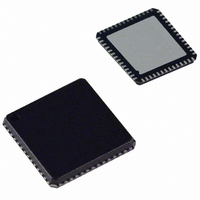
AD8196ACPZ-RL Analog Devices Inc, AD8196ACPZ-RL Datasheet - Page 22

AD8196ACPZ-RL
Manufacturer Part Number
AD8196ACPZ-RL
Description
IC,Telecom Switching Circuit,LLCC,56PIN,PLASTIC
Manufacturer
Analog Devices Inc
Type
HDMI/DVI Switchr
Datasheet
1.AD8196ACPZ-RL.pdf
(24 pages)
Specifications of AD8196ACPZ-RL
Applications
DVI, HDMI Signal Switching
Mounting Type
Surface Mount
Package / Case
56-LFCSP
Lead Free Status / RoHS Status
Lead free / RoHS Compliant
AD8196
maximum allowed voltage on the auxiliary lines. For example,
if the DDC bus is using 5 V I
connected to +5 V relative to DVEE.
In a typical application, all pins labeled AVEE or DVEE should
be connected directly to ground. All pins labeled AVCC,
DVCC, VTTI, or VTTO should be connected to 3.3 V, and
Pin AMUXVCC tied to 5 V. The supplies can also be powered
individually, but care must be taken to ensure that each stage of
the AD8196 is powered correctly.
Power Supply Bypassing
The AD8196 requires minimal supply bypassing. When
powering the supplies individually, place a 0.01 μF capacitor
between each 3.3 V supply pin (AVCC, DVCC, VTTI, and
VTTO) and ground to filter out supply noise. Generally, bypass
capacitors should be placed near the power pins and should
connect directly to the relevant supplies (without long inter-
vening traces). For example, to improve the parasitic inductance
of the power supply decoupling capacitors, minimize the trace
length between capacitor landing pads and the vias as shown in
Figure 34.
Figure 34. Recommended Pad Outline for Bypass Capacitors
2
C, then AMUXVCC should be
RECOMMENDED
NOT RECOMMENDED
EXTRA ADDED INDUCTANCE
Rev. 0 | Page 22 of 24
In applications where the AD8196 is powered by a single 3.3 V
supply, it is recommended to use two reference supply planes
and bypass the 3.3 V reference plane to the ground reference
plane with one 220 pF, one 1000 pF, two 0.01 μF, and one 4.7 μF
capacitors. The capacitors should via down directly to the
supply planes and be placed within a few centimeters of the
AD8196. The AMUXVCC supply does not require additional
bypassing. This scheme is illustrated in Figure 35.
AUXILIARY LINES
TMDS TRACES
Figure 35. Example Placement of Power Supply Decoupling Capacitors
Around the AD8196
AD8196
DECOUPLING
CAPACITORS


