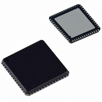
AD8196ACPZ-RL Analog Devices Inc, AD8196ACPZ-RL Datasheet - Page 13

AD8196ACPZ-RL
Manufacturer Part Number
AD8196ACPZ-RL
Description
IC,Telecom Switching Circuit,LLCC,56PIN,PLASTIC
Manufacturer
Analog Devices Inc
Type
HDMI/DVI Switchr
Datasheet
1.AD8196ACPZ-RL.pdf
(24 pages)
Specifications of AD8196ACPZ-RL
Applications
DVI, HDMI Signal Switching
Mounting Type
Surface Mount
Package / Case
56-LFCSP
Lead Free Status / RoHS Status
Lead free / RoHS Compliant
upon reset). If only external terminations are provided (if the
internal terminations are disabled), set the output current level
to 10 mA by programming the TX_OCL bit of the transmitter
settings register. The high speed outputs must be disabled if
there are no output termination resistors present in the system.
The output pre-emphasis can be manually configured to provide
one of four different levels of high frequency boost. The specific
boost level is selected by programming the TX_PE bits of the
transmitter settings register. No specific cable length is suggested
for a particular pre-emphasis setting because cable performance
varies widely between manufacturers.
SWITCHING MODE
The AD8196 behaves like a 2:1 HDMI/DVI link multiplexer by
routing groups of four TMDS input channels to the four channel
output. In this mode, the user selects the group of high speed
source signals (A or B) that is routed to the output by program-
ming the HS_CH bit of the high speeds modes register as
shown in Table 7. The group of low speed auxiliary source
signals (AUX_A or AUX_B) that is routed to the common
output is separately set by programming the AUX_CH bit of
the auxiliary device register as shown in Table 9.
AUXILIARY LINES SWITCHING
The auxiliary (low speed) lines have no amplification. They are
routed using a passive switch that is bandwidth compatible with
standard speed I
connection is shown in Figure 27.
When turning off the AD8196, care needs to be taken with
the AMUXVCC supply to ensure that the auxiliary multiplexer
Figure 27. Auxiliary Channel Simplified Schematic
Showing AUX_A0 to AUX_COM0 Routing
2
C. The schematic equivalent for this passive
AUX_A0
½C
AUX
R
AUX
½C
AUX_COM0
AUX
Rev. 0 | Page 13 of 24
pins are in a high impedance state. A scenario that illustrates
this requirement is one where the auxiliary multiplexer is used
to switch the display data channel (DDC) bus. In some applica-
tions, additional devices can be connected to the DDC bus
(such as an EEPROM with EDID information) upstream of the
AD8196. Extended display identification data (EDID) is a VESA
standard-defined data format for conveying display configuration
information to sources to optimize display use. EDID devices
may need to be available via the DDC bus, regardless of the state
of the AD8196 and any downstream circuit. For this configura-
tion, the auxiliary inputs of the powered down AD8196 need to
be in a high impedance state to avoid pulling down on the DDC
lines and preventing these other devices from using the bus.
When the AD8196 is powered from a simple resistor network,
as shown in Figure 28, it uses the 5 V supply that is required
from any HDMI/DVI source to guarantee high impedance of
the auxiliary multiplexer pins. The AMUXVCC supply does not
draw any static current; therefore, it is recommended that the
resistor network tap the 5 V supplies as close to the connectors
as possible to avoid any additional voltage drop.
This precaution does not need to be taken if the DDC peripheral
circuitry is connected to the bus downstream of the AD8196.
SOURCE A
SOURCE B
PIN 18 HDMI CONNECTOR
PIN 18 HDMI CONNECTOR
PIN 14 DVI CONNECTOR
PIN 14 DVI CONNECTOR
Figure 28. Suggested AMUXVCC Power Scheme
+5V
+5V
PERIPHERAL
PERIPHERAL
CIRCUITRY
CIRCUITRY
I < 50mA
I < 50mA
10kΩ
10kΩ
10MΩ
AMUXVCC
+5V INTERNAL
(IF ANY)
AD8196
AD8196


