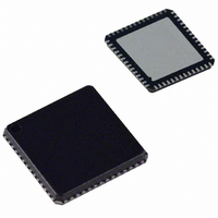
AD8196ACPZ-RL Analog Devices Inc, AD8196ACPZ-RL Datasheet - Page 14

AD8196ACPZ-RL
Manufacturer Part Number
AD8196ACPZ-RL
Description
IC,Telecom Switching Circuit,LLCC,56PIN,PLASTIC
Manufacturer
Analog Devices Inc
Type
HDMI/DVI Switchr
Datasheet
1.AD8196ACPZ-RL.pdf
(24 pages)
Specifications of AD8196ACPZ-RL
Applications
DVI, HDMI Signal Switching
Mounting Type
Surface Mount
Package / Case
56-LFCSP
Lead Free Status / RoHS Status
Lead free / RoHS Compliant
1.
AD8196
SERIAL CONTROL INTERFACE
RESET
On initial power-up, or at any point in operation, the AD8196
register set can be restored to the default values by pulling the
RESET pin to low according to the specification in Table 1.
During normal operation, however, the RESET pin must be
pulled up to 3.3 V. Pulling the RESET pin to low sets the
HS_CH register to 0 (Input A) and incurs the associated
switching delay before the input can be switched to Input B,
regardless of the previous state of the AD8196.
WRITE PROCEDURE
To write data to the AD8196 register set, an I
a microcontroller) needs to send the appropriate control signals
to the AD8196 slave device. The signals are controlled by the
I
procedure, see Figure 29. The steps for a write procedure are as
follows:
2.
3.
4.
5.
2
C master, unless otherwise specified. For a diagram of the
Send a start condition (while holding the I2C_SCL line
high, pull the I2C_SDA line low).
Send the AD8196 part address (seven bits). The upper six
bits of the AD8196 part address are the static value [100100]
and the LSB is set by Input Pin I2C_ADDR. This transfer
should be MSB first.
Send the write indicator bit (0).
Wait for the AD8196 to acknowledge the request.
Send the register address (eight bits) to which data is to be
written. This transfer should be MSB first.
GENERAL CASE
EXAMPLE
I2C_SDA
I2C_SDA
I2C_SCL
*THE SWITCHING/UPDATE DELAY BEGINS AT THE FALLING EDGE OF THE
LAST DATA BIT; FOR EXAMPLE, THE FALLING EDGE JUST BEFORE STEP 8.
START
1
2
FIXED ADDR PART
2
C master (such as
ADDR
R/W
3
ACK
Figure 29. I
4
Rev. 0 | Page 14 of 24
5
2
C Write Procedure
REGISTER ADDR
6.
7.
8.
9.
Wait for the AD8196 to acknowledge the request.
Send the data (eight bits) to be written to the register
whose address was set in Step 5. This transfer should be
MSB first.
Wait for the AD8196 to acknowledge the request.
Do one of the following:
a.
b.
c.
d.
Send a stop condition (while holding the I2C_SCL
line high, pull the I2C_SDA line high) and release
control of the bus to end the transaction (shown in
Figure 29).
Send a repeated start condition (while holding the
I2C_SCL line high, pull the I2C_SDA line low) and
continue with Step 2 in this procedure to perform
another write.
Send a repeated start condition (while holding the
I2C_SCL line high, pull the I2C_SDA line low) and
continue with Step 2 of the read procedure (in the
Read Procedure section) to perform a read from
another address.
Send a repeated start condition (while holding the
I2C_SCL line high, pull the I2C_SDA line low) and
continue with Step 8 of the read procedure (in the
Read Procedure section) to perform a read from the
same address set in Step 5.
ACK
6
7
DATA
*
ACK
8
STOP
9


