AD8156ABCZ Analog Devices Inc, AD8156ABCZ Datasheet - Page 16
AD8156ABCZ
Manufacturer Part Number
AD8156ABCZ
Description
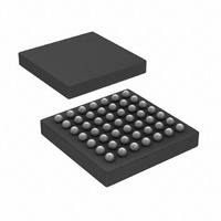
IC,Telecom Switching Circuit,BGA,49PIN,PLASTIC
Manufacturer
Analog Devices Inc
Series
XStream™r
Datasheet
1.AD8156ABCZ.pdf
(20 pages)
Specifications of AD8156ABCZ
Applications
4 x 4 Crosspoint Switch
Interface
LVTTL, LVCMOS
Voltage - Supply
3 V ~ 3.6 V
Package / Case
49-CSPBGA
Mounting Type
Surface Mount
Lead Free Status / RoHS Status
Lead free / RoHS Compliant
Available stocks
Company
Part Number
Manufacturer
Quantity
Price
Company:

Part Number:
AD8156ABCZ
Manufacturer:
Analog Devices Inc
Quantity:
10 000


AD8156
ADDRESS PINS, A[3:0] INPUTS
The AD8156 feature sets can be set port by port or globally.
A[3:2] specify what is being programmed or read back when
the part is being configured port by port. Connectivity, output
current, equalization, or global programming features are
chosen based on the values of A[3:2]. Similarly, A[1:0] address
the port that is being programmed or read back. In global
programming, A[1:0] serve a different function. Refer to Table 9
to Table 15 for programming examples.
Table 7. Dual 2 × 2 Mode Programming Table
Address A[3:0]
Input A3 to Input A0 enable Output 3 to Output 0, respectively.
Table 8. 4 × 4 Mode Programming Table
Mode
Write/Read Connectivity
and Disable
Write/Read Output
Current Level
Broadcast
Connectivity/Disable
Broadcast Output
Current Level
Broadcast EQ Setting
Program EQ Setting
1 = Enables the output (for all A[3:0] inputs)
0 = Disables the output (for all A[3:0] inputs)
Address A[3:0]
0 0 A1 A0
A1 and A0 determine which
output is being programmed.
0 1 A1 A0
A1 and A0 determine which
output is being programmed.
1 0 0 0
1 0 0 1
1 0 1 1
1 1 A1 A0
A1 and A0 determine which
input is being programmed.
Rev. 0 | Page 16 of 20
Data D[3:0]
Input D3 to Input D0 control the connectivity of Output 3 to Output 0, respectively.
0 = Input 2, 1 = Input 3 (for D2 and D3)
0 = Input 0, 1 = Input 1 (for D0 and D1)
Data D[3:0]
0 D2 D1 D0
D1 and D0 determine which input is connected to which output;
D2 determines the enabled/disabled state of that output, with D2 = 1
(enable). When writing or reading, D3 is always 0.
D3 D2 D1 D0
D0 to D3 binarily program the output current level/voltage swing with the
output current = 2 mA + (2 mA × decimal (D[3:0])).
0 D2 D1 D0
D1 and D0 determine which input is connected to all of the outputs.
D2 determines the enabled/disabled state of all outputs with D2 = 1 (enable).
When writing or reading, D3 is always 0.
D3 D2 D1 D0
D0 to D3 binarily program the output current level/voltage swing with the
output current = 2 mA + (2 mA × decimal (D[3:0])). The value is written to
all outputs.
D3 D2 D1 D0
Data inputs D0 to D3 set the input equalization level where:
Gain(f ) = D[3:0]/15 × 40 log
D3 D2 D1 D0
D0 to D3 set the input equalization level, where:
Gain(f ) = D[3:0]⁄15 × 40 log
DATA PINS, D[3:0] INPUTS/OUTPUTS
In readback mode, the D[3:0] pins are low impedance outputs
indicating the stored values in the memory to be read. The
readback drivers are designed to drive high impedances only,
so external drivers connected to D[3:0] must be disabled during
readback mode.
CONTROL INTERFACE LEVELS
The AD8156 control interface shares the data path supply pins,
V
V
more than 3.7 V. Regardless of supply, the logic threshold is
approximately one-half the supply range, allowing the interface
to be used with most LVCMOS- and LVTTL-logic drivers.
CC
CC
and V
and the negative supply V
EE
. The potential between the positive logic supply
10
10
(f/0.83 GHz).
(f⁄0.83 GHz).
EE
must be at least 3.0 V and no
Related parts for AD8156ABCZ
Image
Part Number
Description
Manufacturer
Datasheet
Request
R

Part Number:
Description:
SENSOR GAS FOR CO/NO2 EXHAUST
Manufacturer:
GE Sensing
Datasheet:

Part Number:
Description:
±1.7g Dual-Axis IMEMS Accelerometer Evaluation Board
Manufacturer:
Analog Devices Inc
Datasheet:

Part Number:
Description:
Inertial Sensor Evaluation System
Manufacturer:
Analog Devices Inc
Datasheet:
Part Number:
Description:
Manufacturer:
Analog Devices Inc
Datasheet:
Part Number:
Description:
Manufacturer:
Analog Devices Inc
Datasheet:
Part Number:
Description:
Manufacturer:
Analog Devices Inc
Datasheet:
Part Number:
Description:
Manufacturer:
Analog Devices Inc
Datasheet:
Part Number:
Description:
Manufacturer:
Analog Devices Inc
Datasheet:
Part Number:
Description:
Manufacturer:
Analog Devices Inc
Datasheet:
Part Number:
Description:
Manufacturer:
Analog Devices Inc
Datasheet:
Part Number:
Description:
Manufacturer:
Analog Devices Inc
Datasheet:
Part Number:
Description:
Manufacturer:
Analog Devices Inc
Datasheet:
Part Number:
Description:
Manufacturer:
Analog Devices Inc
Datasheet: