AD8156ABCZ Analog Devices Inc, AD8156ABCZ Datasheet - Page 15
AD8156ABCZ
Manufacturer Part Number
AD8156ABCZ
Description
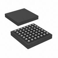
IC,Telecom Switching Circuit,BGA,49PIN,PLASTIC
Manufacturer
Analog Devices Inc
Series
XStream™r
Datasheet
1.AD8156ABCZ.pdf
(20 pages)
Specifications of AD8156ABCZ
Applications
4 x 4 Crosspoint Switch
Interface
LVTTL, LVCMOS
Voltage - Supply
3 V ~ 3.6 V
Package / Case
49-CSPBGA
Mounting Type
Surface Mount
Lead Free Status / RoHS Status
Lead free / RoHS Compliant
Available stocks
Company
Part Number
Manufacturer
Quantity
Price
Company:

Part Number:
AD8156ABCZ
Manufacturer:
Analog Devices Inc
Quantity:
10 000


CONTROL INTERFACE DESCRIPTION
The control interface for the AD8156 consists of a set of
address, data, and several control pins. All control pins are
active low. The control interface is level sensitive.
CONTROL PINS
All control pins on the chip are level-sensitive, not edge-triggered.
The preferred programming method is to assert the data and
address pins to their desired configuration, wait one control bit
period, then pull WE low to write to the first bank of registers.
After one control bit period, WE is pulled high. After an
additional control bit period, the address and data pins can be
set to their next values, and the cycle repeats. Using this
method, each write takes three control bit periods.
After the first bank of registers is programmed, UPD is pulled low,
which transfers the data from the first bank of latches to the second
bank of latches. When UPD is pulled low, the full chip updates,
regardless of the status of the address, data, WE , or RE pins.
Writing to the part while UPD is pulled low writes through the
first bank of registers and into the second bank, immediately
affecting the connectivity and output current of the part. It is
recommended that the user write to the first bank with one data
bit cycle, and subsequently activate the UPD pin low, because
data and address pin skews presented to the part can lead to
errors when writing through both banks simultaneously. If
skews are properly controlled, a transparent write can allow a
very quick change of states in 4 × 4 mode.
RST Pin
At any time, a reset pulse to RST can be applied to the control
interface to globally reset all first and second bank latches to
their default values. The device has an internal power-on reset
circuit, but it is recommended that RST be held low during
power-up. The default values for the chip include disabling all
outputs, turning off equalization, and setting output current code to
the default, b0111 (16 mA). The default connection is the buffer
state, or IN0 → OUT0, IN1 → OUT1, IN2 → OUT2, IN3 → OUT3;
Table 6. Basic Control Pin Functions
RST
1
0
1
1
1
1
1
1
CS
1
x
0
0
0
0
0
0
MODE
x
x
0
0
0
0
0
1
WE
x
x
1
0
1
1
0
x
RE
x
x
1
1
0
x
x
x
UPD
x
x
1
1
1
0
0
x
Function
Control Interface Disabled. Prior settings are stored, and the chip is run based on the
configuration data stored (in 4 × 4 mode) or set (in dual 2 × 2 mode) previously.
Global Reset. Disables all outputs and equalizers. Output current code set to 0111 (16 mA).
4 × 4 Mode. Address and data pins are ignored (values in the AD8156 memory control connectivity,
output current, and EQ setting).
Write Enable. Writes to the first bank of registers.
Readback Enable. Reads back data on D[3:0] from the addressed latch (second bank of registers).
Global Update. Transfers data from first bank of registers to second bank of registers (active set).
Chip functions update.
Transparent Write. Writes and updates simultaneously through first bank to the second bank of
registers. Chip functions update.
Dual 2 × 2 Mode. Address and data pins asynchronously control the device.
Rev. 0 | Page 15 of 20
all outputs are connected but disabled. RST overrides all of the
other control pins.
CS Pin
The chip select pin, an active low signal, facilitates multiple chip
address decoding. All control signals, except the reset signal, are
ignored when CS is pulled high. The pin disables the control signals
and does not affect operation of the chip. CS does not power down
any of the latches, preserving any data programmed in the latches.
MODE Pin
The MODE pin sets the part in 4 × 4 mode or dual 2 × 2 mode.
Pulling MODE low sets the part in 4 × 4 mode, and pulling
MODE high sets the part in dual 2 × 2 mode. In dual 2 × 2
mode, the WE , RE , and UPD pins are unused.
WE Pin
This pin is the write enable to the first bank of registers. Forcing
WE to logic low allows the data on the D[3:0] pins to be stored
in the first bank of latches for the function specified by A[3:0].
The WE pin must be returned to logic high state before
changing the other pins after a write cycle to avoid overwriting
the first bank data.
UPD Pin
This pin is the write enable to the second bank of registers.
Forcing UPD to logic low transfers the data stored in all first
bank latches to the second bank latches, which is the active set
of registers. The chip functions update during this operation.
RE Pin
This pin is the read enable for the second bank of registers.
Forcing RE to logic low enables the on-chip drivers to drive the
bidirectional D[3:0] pins. The on-chip drivers are only intended
to drive high impedance loads, so any external drivers of D[3:0]
must be disabled when RE is low.
AD8156
Related parts for AD8156ABCZ
Image
Part Number
Description
Manufacturer
Datasheet
Request
R

Part Number:
Description:
SENSOR GAS FOR CO/NO2 EXHAUST
Manufacturer:
GE Sensing
Datasheet:

Part Number:
Description:
±1.7g Dual-Axis IMEMS Accelerometer Evaluation Board
Manufacturer:
Analog Devices Inc
Datasheet:

Part Number:
Description:
Inertial Sensor Evaluation System
Manufacturer:
Analog Devices Inc
Datasheet:
Part Number:
Description:
Manufacturer:
Analog Devices Inc
Datasheet:
Part Number:
Description:
Manufacturer:
Analog Devices Inc
Datasheet:
Part Number:
Description:
Manufacturer:
Analog Devices Inc
Datasheet:
Part Number:
Description:
Manufacturer:
Analog Devices Inc
Datasheet:
Part Number:
Description:
Manufacturer:
Analog Devices Inc
Datasheet:
Part Number:
Description:
Manufacturer:
Analog Devices Inc
Datasheet:
Part Number:
Description:
Manufacturer:
Analog Devices Inc
Datasheet:
Part Number:
Description:
Manufacturer:
Analog Devices Inc
Datasheet:
Part Number:
Description:
Manufacturer:
Analog Devices Inc
Datasheet:
Part Number:
Description:
Manufacturer:
Analog Devices Inc
Datasheet: