AD8156ABCZ Analog Devices Inc, AD8156ABCZ Datasheet - Page 13
AD8156ABCZ
Manufacturer Part Number
AD8156ABCZ
Description
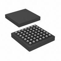
IC,Telecom Switching Circuit,BGA,49PIN,PLASTIC
Manufacturer
Analog Devices Inc
Series
XStream™r
Datasheet
1.AD8156ABCZ.pdf
(20 pages)
Specifications of AD8156ABCZ
Applications
4 x 4 Crosspoint Switch
Interface
LVTTL, LVCMOS
Voltage - Supply
3 V ~ 3.6 V
Package / Case
49-CSPBGA
Mounting Type
Surface Mount
Lead Free Status / RoHS Status
Lead free / RoHS Compliant
Available stocks
Company
Part Number
Manufacturer
Quantity
Price
Company:

Part Number:
AD8156ABCZ
Manufacturer:
Analog Devices Inc
Quantity:
10 000


THEORY OF OPERATION
The AD8156 is a 4 × 4 crosspoint switch with programmable
input equalization and programmable output current levels. It
can be used as a nonblocking and fully programmable 4 × 4
crosspoint switch, or as a dual 2 × 2 protection switch with fast
channel switching. Each lane can run at any rate from dc to
6.25 Gbps independent of the other lanes.
In 4 × 4 mode, the user writes the control data to double-latched
memory cells through a simple CPU interface. Connectivity,
individual output disables, output current level, and input equali-
zation are all individually programmable. Broadcast addresses
can be used to simultaneously program the functionality of all
channels. A global reset disables the part and resets all equalizers
and output current levels to their default states. A chip select
pin can be used in applications where a single bus is controlling
multiple switches.
When in dual 2 × 2 mode, the part functions as two individual
2 × 2 switches whose connectivity is asynchronously controlled
by the D3 to D0 pins, and output enable is controlled by the A3
to A0 pins. The dual 2 × 2 mode allows for sub-10 ns output
channel switching or output enable. Output swing control and
input equalization cannot be controlled in dual 2 × 2 mode
because all the data and address pins are used as asynchronous
control pins. However, settings are retained when switching modes,
so the user can set the desired swing and input equalization settings
in 4 × 4 mode on startup and then switch to dual 2 × 2 mode.
The user can switch at will between 4 × 4 mode and dual 2 × 2
mode by toggling the MODE pin. When switching from 4 × 4
mode to dual 2 × 2 mode, EQ and output current settings are
retained, but the output connectivity control is instantly
switched to the asynchronous interface of A[3:0] and D[3:0].
To have uninterrupted data flow when switching from 4 × 4
mode to dual 2 × 2 mode, the address and data pins should be
set into the desired states for dual 2 × 2 mode before changing
the MODE pin. When switching from dual 2 × 2 mode to 4 × 4
mode, EQ and the output current settings are also retained, but
the connectivity specified by the values of A[3:0] and D[3:0]
when MODE went low are retained in memory. Until some
other connectivity is set using the 4 × 4 control interface, the
last dual 2 × 2 mode settings are stored in memory.
4 × 4 MODE
Pulling the MODE pin low puts the AD8156 in 4 × 4 mode. In
this mode, the chip is controlled by the values stored in the on-
chip memory. This memory is organized as two banks of latches;
the second bank controls the chip, and the first bank allows the
next set of configuration data to be written while the chip is operat-
ing based on the second bank data. To write to the first bank of
memory, the user sets data and address to the desired states and
pulls WE low. This writing process is repeated until all desired
configuration data is stored in the first bank of latches, and then the
chip configuration is simultaneously updated by pulling UPD low.
Rev. 0 | Page 13 of 20
If desired for verification, the value of the second bank of
latches can be read back by pulling RE low. When RE is low,
Data Pin D3 to Data Pin D0 are driven by the chip. The timing
of this operation is shown in Figure 5. Because the interface is
entirely asynchronous, the only limitation on the timing of the
read cycle is that each period must be a minimum of 15 ns.
Connectivity Control
Connection between an output and an input is set by addressing
a specific output and connecting it to an input. Each output has
a disable bit. Table 10 shows how to set the crosspoint
connectivity.
Output Current Control
Output current is controlled by addressing a specific output and
choosing the output current. The output current is equal to
For example, the default code for D[3:0] is b0111. Therefore, the
output current level is 2 mA + (2 mA × 7) = 16 mA. Table 11 and
Table 13 show how to set the output current levels.
Input Equalization Control
Input equalization is set per input lane. The equalization is
set in ~1.53 dB steps, from 0 dB to 23 dB of equalization at
3.125 GHz (roughly corresponding to a 6.25 Gbps bit rate).
The amount of equalization is
A value of 0000 disables the equalizer, saving power.
Global Setting
By writing to one of three broadcast addresses, the user can set
all connectivity, output current, or input equalization settings to
the same value. Broadcast addresses are controlled similarly to
other control addresses. See Table 12, Table 13, and Table 14 for
broadcast mode programming.
DUAL 2 × 2 MODE
Pulling the MODE pin high puts the AD8156 in dual 2 × 2
mode. In this mode, the part is asynchronously controlled by
the address and data pins, A[3:0] and D[3:0], respectively. In
dual 2 × 2 mode, the switch is configured as two individual 2 × 2
switches, and each output can be individually disabled. OUT0
and OUT1 can be connected to either IN0 or IN1, and OUT2
and OUT3 can connect to either IN2 or IN3. There are no
connectivity options in dual 2 × 2 mode to connect OUT0/OUT1
to IN2/IN3, or OUT2/OUT3 to IN0/IN1.
In dual 2 × 2 mode, input equalization and output level settings
are not accessible. If these functions are needed, the user should
program these functions in 4 × 4 mode and then return to dual
2 × 2 mode. Output swing and equalization settings are retained
from 4 × 4 mode to dual 2 × 2 mode. Readback is not available
in dual 2 × 2 mode.
2 mA + (2 mA × D[3:0])
gain
(
f
)
=
D[3:0]
15
×
40
log
10
. 0
83
f
GHz
AD8156
Related parts for AD8156ABCZ
Image
Part Number
Description
Manufacturer
Datasheet
Request
R

Part Number:
Description:
SENSOR GAS FOR CO/NO2 EXHAUST
Manufacturer:
GE Sensing
Datasheet:

Part Number:
Description:
±1.7g Dual-Axis IMEMS Accelerometer Evaluation Board
Manufacturer:
Analog Devices Inc
Datasheet:

Part Number:
Description:
Inertial Sensor Evaluation System
Manufacturer:
Analog Devices Inc
Datasheet:
Part Number:
Description:
Manufacturer:
Analog Devices Inc
Datasheet:
Part Number:
Description:
Manufacturer:
Analog Devices Inc
Datasheet:
Part Number:
Description:
Manufacturer:
Analog Devices Inc
Datasheet:
Part Number:
Description:
Manufacturer:
Analog Devices Inc
Datasheet:
Part Number:
Description:
Manufacturer:
Analog Devices Inc
Datasheet:
Part Number:
Description:
Manufacturer:
Analog Devices Inc
Datasheet:
Part Number:
Description:
Manufacturer:
Analog Devices Inc
Datasheet:
Part Number:
Description:
Manufacturer:
Analog Devices Inc
Datasheet:
Part Number:
Description:
Manufacturer:
Analog Devices Inc
Datasheet:
Part Number:
Description:
Manufacturer:
Analog Devices Inc
Datasheet: