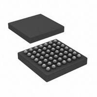
AD8156ABCZ Analog Devices Inc, AD8156ABCZ Datasheet

AD8156ABCZ
Specifications of AD8156ABCZ
Available stocks
Related parts for AD8156ABCZ
AD8156ABCZ Summary of contents
Page 1
FEATURES 4 × 4, fully differential, nonblocking array Configurable for dual 2 × 2 operation DC to 6.25 Gbps per channel, NRZ data rate Programmable input equalization compensates for over 40” of FR-4 at 6.25 Gbps Multicast and broadcast modes ...
Page 2
AD8156 TABLE OF CONTENTS Features .............................................................................................. 1 Applications....................................................................................... 1 Functional Block Diagram .............................................................. 1 General Description ......................................................................... 1 Revision History ............................................................................... 2 Specifications..................................................................................... 3 Electrical Specifications............................................................... 3 Timing Specifications .................................................................. 4 Timing Diagrams.............................................................................. 5 Absolute Maximum Ratings............................................................ 7 Thermal Resistance ...
Page 3
SPECIFICATIONS ELECTRICAL SPECIFICATIONS 3 TTI TTO p-p differential 25°C, unless otherwise noted Table 1. Parameter DYNAMIC PERFORMANCE ...
Page 4
AD8156 TIMING SPECIFICATIONS 3 TTI TTO p-p differential 25°C, unless otherwise noted Table 2. Parameter FIRST RANK ...
Page 5
TIMING DIAGRAMS CS WE A[3:0] D[3:0] CS UPD OUTxN/P ENABLE OUTxN/P DISABLE OUTxN/P TOGGLE t CSW ASW DSW AHW t t DHW WP Figure 2. First Rank Write Cycle t t CSU UW t UOE t UOD ...
Page 6
AD8156 CS UPD WE OUTxN/P ENABLE OUTxN/P DISABLE OUTxN/P TOGGLE CS RE ADDR[3:0] DATA[3:0] RST OUTxN/P DISABLE t t WOE WHU t WOD t WOT Figure 4. Transparent Write and Update Cycle ADDR1 ADDR2 DATA1 DATA2 CSR ...
Page 7
ABSOLUTE MAXIMUM RATINGS Table 3. Parameter Rating 3 0.6 V TTI 0.6 V TTO CC 1 Internal Power Dissipation 1.92 W Input Voltage V + 0.6 V ...
Page 8
AD8156 PIN CONFIGURATIONS AND FUNCTION DESCRIPTIONS V CC OUT0P OUT0N V TTO OUT1P OUT1N V EE Table 5. Pin Function Descriptions Pin No. Mnemonic Description A1 V Negative Supply IN1N High Speed Input Complement. A3 IN1P High Speed ...
Page 9
TYPICAL PERFORMANCE CHARACTERISTICS 3 TTI TTO p-p differential 25°C, unless otherwise noted 50ps/DIV Figure 8. Input Eye ...
Page 10
AD8156 25ps/DIV Figure 14. Input Eye Diagram at 6.25 Gbps, 40” FR4 6.25Gbps 15 10 3.2Gbps 0.5 1.0 1.5 DIFFERENTIAL INPUT (V p-p) Figure 15. Deterministic Jitter vs. Input Signal Level (No EQ) ...
Page 11
V (V) CC Figure 20. Deterministic Jitter vs 0.5 1.0 1.5 ...
Page 12
AD8156 TEST CIRCUIT 50Ω CABLES 2 DATA OUT PATTERN DIFFERENTIAL STRIPLINE TRACES GENERATOR AND 8mils DIELECTRIC HEIGHT TRACE LENGTHS = 10", 20", 30", AND 40" *SINGLE-ENDED REPRESENTATION AD8156 AC-COUPLED 50Ω EVALUATION BOARD CABLES FR4 TEST IN0P/N OUT0P/N ...
Page 13
THEORY OF OPERATION The AD8156 × 4 crosspoint switch with programmable input equalization and programmable output current levels. It can be used as a nonblocking and fully programmable 4 × 4 crosspoint switch dual ...
Page 14
AD8156 When in dual 2 × 2 mode, the A[3:0] and D[3:0] pins set the AD8156 configuration state when CS is low. This configuration method allows the user to have multiple AD8156s share the control bus while each device has ...
Page 15
CONTROL INTERFACE DESCRIPTION The control interface for the AD8156 consists of a set of address, data, and several control pins. All control pins are active low. The control interface is level sensitive. CONTROL PINS All control pins on the chip ...
Page 16
AD8156 ADDRESS PINS, A[3:0] INPUTS The AD8156 feature sets can be set port by port or globally. A[3:2] specify what is being programmed or read back when the part is being configured port by port. Connectivity, output current, equalization, or ...
Page 17
PROGRAMMING EXAMPLES A[3:0] D[3:0] WE UPD Figure 25. Sample Timing Diagram for 4x4 Mode Programming Examples DUAL 2 × 2 MODE (MODE PIN = 1) PROGRAMMING EXAMPLES Table 9. Dual 2 × 2 Mode Programming Address Pins Data Pins A3 ...
Page 18
AD8156 Table 12. Broadcast Connectivity Programming, A[3:0] = b1000 Address Pins Data Pins Table 13. Broadcast ...
Page 19
... OUTLINE DIMENSIONS TOP VIEW DETAIL A * 1.85 1.71 1.50 * COMPLIANT WITH JEDEC STANDARDS MO-192-ABB-1 ORDERING GUIDE Model Temperature Range 1 AD8156ABCZ −40°C to +85°C 1 AD8156-EVALZ RoHS Compliant Part. 8.20 8. BALL A1 PAD CORNER 6.00 BSC SQ BOTTOM 1.00 BSC DETAILA 0.25 MIN ...
Page 20
AD8156 NOTES © 2007 Analog Devices, Inc. All rights reserved. Trademarks and registered trademarks are the property of their respective owners. D06305-0-5/07(0) Rev Page ...


