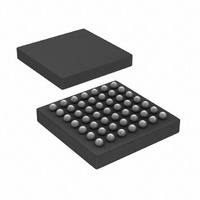
AD8156ABCZ Analog Devices Inc, AD8156ABCZ Datasheet - Page 14

AD8156ABCZ
Manufacturer Part Number
AD8156ABCZ
Description
IC,Telecom Switching Circuit,BGA,49PIN,PLASTIC
Manufacturer
Analog Devices Inc
Series
XStream™r
Datasheet
1.AD8156ABCZ.pdf
(20 pages)
Specifications of AD8156ABCZ
Applications
4 x 4 Crosspoint Switch
Interface
LVTTL, LVCMOS
Voltage - Supply
3 V ~ 3.6 V
Package / Case
49-CSPBGA
Mounting Type
Surface Mount
Lead Free Status / RoHS Status
Lead free / RoHS Compliant
Available stocks
Company
Part Number
Manufacturer
Quantity
Price
Company:
Part Number:
AD8156ABCZ
Manufacturer:
Analog Devices Inc
Quantity:
10 000
AD8156
When in dual 2 × 2 mode, the A[3:0] and D[3:0] pins set the
AD8156 configuration state when CS is low. This configuration
method allows the user to have multiple AD8156s share the control
bus while each device has its own dedicated CS control signal.
INPUT EQUALIZATION
The AD8156 input equalization is an active scheme that is fully
linear over all operating ranges. The useful range of equalization
covers dc to 3.125 GHz frequencies or dc to 6.25 Gbps data
rates. Other key features include:
•
•
IN0P/N
IN1P/N
IN2P/N
IN3P/N
VCC
15 steps of gain, linear in dB, programmable through the
4 × 4 control interface
Gain has a 40 dB per decade slope
RECEIVERS
MODE
INPUT
Figure 24. AD8156 in Dual 2 × 2 Mode
EQUALIZATION
INPUT
EQ
EQ
EQ
EQ
AD8156
SWITCH
SWITCH
2 × 2
2 × 2
DRIVERS
OUTPUT
OUT0P/N
OUT1P/N
OUT2P/N
OUT3P/N
Rev. 0 | Page 14 of 20
•
•
•
•
As with all equalizers, the gain setting is the key. The ideal
method of choosing the proper gain setting is to run the equalizer
with the channel, and choose the setting with minimum jitter.
If this process is not possible or is too time consuming for the
number of channels required, the loss of the channel at
3.125 GHz should be measured. The best equalizer setting is
usually 2 dB to 4 dB more than the loss at 3.125 GHz. Using the
40 dB slope of the equalizer gain, the gain at other frequencies
can be calculated based on the peak gain at 3.125 GHz. The
formula to use is
where f is the fundamental frequency of the data, or the data
rate divided by 2 (that is, 6.25 Gbps → f = 3.125 GHz).
Performance of the equalizer is heavily dependent on the channel
used. Operation at high speeds depends on features such as
dielectric used (for example, FR4, Nelco3000, or Rogers), connector
quality, via stub length, and routing geometry and topology.
Peak gain of 23 dB at 3.125 GHz (~6.25 Gbps)
Equalizes more than 40” of typical FR4 backplane with
associated connectors and vias at all speeds
0.10 UI p-p residual deterministic jitter typ @ 3.125 Gbps
0.15 UI p-p residual deterministic jitter typ @ 6.25 Gbps
gain
(
f
)
=
D[3:0]
15
×
40
log
10
. 0
83
f
GHz


