DLP-245SY-G-C DLP Design Inc, DLP-245SY-G-C Datasheet - Page 13
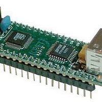
DLP-245SY-G-C
Manufacturer Part Number
DLP-245SY-G-C
Description
Interface Modules & Development Tools USB/Micro Dev Board W/GRICH C COMPILER
Manufacturer
DLP Design Inc
Datasheet
1.DLP-245SY-G-C.pdf
(15 pages)
Specifications of DLP-245SY-G-C
Interface Type
USB
Data Bus Width
8 bit
Operating Supply Voltage
5 V
Product
Interface Modules
For Use With/related Products
SX48
Lead Free Status / RoHS Status
Lead free / RoHS Compliant


13
14
15
16
17
18
19
20
21
22
23
24
25
26
27
28
29
30
31
32
33
34
35
36
37
38
39
GROUND
3V3OUT
internal 3.3v supply to the USB transceiver cell and the RSTOUT# pin. A small amount of current
(<=5mA) can be drawn from this pin to power external 3.3v logic if required.
GROUND
SWVCC
and Q1 MOSFET power switch. R5 and C3 control the power-up rate to help limit inrush current.
GROUND
VCC-IO
When interfacing with 3.3v external logic, connect VCC-IO to the 3.3v supply of the external logic;
otherwise, connect to the VCC to drive out at 5v CMOS level. This pin must be connected to VCC
from the target electronics or EXTVCC.
EXTVCC
PORTVCC if the module is to be powered by the USB port (typical configuration).
PORTVCC
USB port (typical configuration). 500mA is the maximum current available to the DLP-245SY and
target electronics if the USB device is configured for high power.
DB7
DB6
DB5
DB4
DB3
DB2
DB1
DB0
E0
E1
E2
E3
E4
E5
E6
E7
B3
B2
B1
(I/O) Port Pin E0 connected to the SX48 microcontroller.
(I/O) Port Pin E1 connected to the SX48 microcontroller.
(I/O) Port Pin E2 connected to the SX48 microcontroller.
(I/O) Port Pin E3 connected to the SX48 microcontroller.
(I/O) Port Pin E4 connected to the SX48 microcontroller.
(I/O) Port Pin E5 connected to the SX48 microcontroller.
(I/O) Port Pin E6 connected to the SX48 microcontroller.
(I/O) Port Pin E7 connected to the SX48 microcontroller.
(I/O) Port Pin B3 connected to the SX48 microcontroller.
(I/O) Port Pin B2 connected to the SX48 microcontroller.
(I/O) Port Pin B1 connected to the SX48 microcontroller.
(I/O) Line 7 of the data bus between the SX48 and the FT245BM USB-FIFO.
(I/O) Line 6 of the data bus between the SX48 and the FT245BM USB-FIFO.
(I/O) Line 5 of the data bus between the SX48 and the FT245BM USB-FIFO.
(I/O) Line 4 of the data bus between the SX48 and the FT245BM USB-FIFO.
(I/O) Line 3 of the data bus between the SX48 and the FT245BM USB-FIFO.
(I/O) Line 2 of the data bus between the SX48 and the FT245BM USB-FIFO.
(I/O) Line 1 of the data bus between the SX48 and the FT245BM USB-FIFO.
(I/O) Line 0 of the data bus between the SX48 and the FT245BM USB-FIFO.
(In) 3.0 volt to +5.25 volt VCC to the FT245BM’s interface pins 10-12, 14-16, and 18-25.
(Out) Power from EXTVCC (Pin 19) controlled via Pin 10 (POWERN#) of the FT245BM
(Out) Output from the integrated L.D.O. regulator. Its primary purpose is to provide the
(In) Use for applying main power (4.4 to 5.25 volts) to the module. Connect to
(Out) Power from USB port. Connect to EXTVCC if module is to be powered by the
13
Related parts for DLP-245SY-G-C
Image
Part Number
Description
Manufacturer
Datasheet
Request
R

Part Number:
Description:
RF Development Tools DLP-RFS1231 development kit
Manufacturer:
DLP Design
Datasheet:

Part Number:
Description:
MODULE USB-TO-TTL SRL UART CONV
Manufacturer:
DLP Design Inc
Datasheet:

Part Number:
Description:
Zigbee / 802.15.4 Modules & Development Tools USE 626-DLP-RF2-Z
Manufacturer:
DLP Design Inc
Datasheet:

Part Number:
Description:
Interface Modules & Development Tools FLASH2 TARGET BOARD 18F2321 w/IDE 2k Ltd
Manufacturer:
DLP Design Inc

Part Number:
Description:
Interface Modules & Development Tools FLASH2 TARGET BOARD 16F917 w/IDE 2k Ltd
Manufacturer:
DLP Design Inc

Part Number:
Description:
Interface Modules & Development Tools FLASH2 TARGET BOARD 18F4420 w/IDE 2k Ltd
Manufacturer:
DLP Design Inc
Part Number:
Description:
Zigbee / 802.15.4 Modules & Development Tools TTL SERIAL INTERFACE MODULE
Manufacturer:
DLP Design Inc
Datasheet:
Part Number:
Description:
Zigbee / 802.15.4 Modules & Development Tools TTL SERIAL INTERFACE MODULE
Manufacturer:
DLP Design Inc
Datasheet:
Part Number:
Description:
Interface Modules & Development Tools USB FPGA Module w/ Xilinx XC3S400A
Manufacturer:
DLP Design Inc
Datasheet:

Part Number:
Description:
Interface Modules & Development Tools Dual Ch USB Adapter w/ FTDI FT2232H
Manufacturer:
DLP Design Inc
Datasheet:

Part Number:
Description:
MODULE USB-MCU FT245RL W/16F877A
Manufacturer:
DLP Design Inc
Datasheet:

Part Number:
Description:
MODULE USB-TO-FPGA TRAINING TOOL
Manufacturer:
DLP Design Inc
Datasheet:

Part Number:
Description:
MODULE USB-MCU FT232R W/18F2410
Manufacturer:
DLP Design Inc
Datasheet:

Part Number:
Description:
MODULE USB-MCU FT245RL W/SX48
Manufacturer:
DLP Design Inc
Datasheet:

Part Number:
Description:
MODULE USB-MCU FT2232D W/16F877A
Manufacturer:
DLP Design Inc
Datasheet: