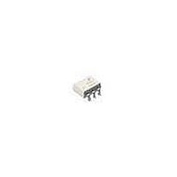
MOC3052SR2M Fairchild Semiconductor, MOC3052SR2M Datasheet - Page 5

MOC3052SR2M
Manufacturer Part Number
MOC3052SR2M
Description
Triac & SCR Output Optocouplers 6Pin 600V Optocoupl Rand Phs Triac Drvr
Manufacturer
Fairchild Semiconductor
Datasheet
1.MOC3052M_F132.pdf
(13 pages)
Specifications of MOC3052SR2M
Configuration
1
Maximum Input Current
60 mA
Maximum Operating Temperature
+ 85 C
Maximum Power Dissipation
330 mW
Maximum Reverse Diode Voltage
3 V
Minimum Operating Temperature
- 40 C
Output Type
AC
Package / Case
PDIP SMD White
Typical Input Voltage
1.15 V
Zero-crossing Circuit
No
Output Device
Triac
Isolation Voltage
5250 Vrms
Peak Output Voltage (vdrm)
600 V
Maximum Input Voltage
1.5 V
Maximum Output Voltage
420 VAC
Minimum Trigger Current
10 mA (Max)
Lead Free Status / RoHS Status
Lead free / RoHS Compliant
Other names
MOC3052SR2M_NL
Available stocks
Company
Part Number
Manufacturer
Quantity
Price
Company:
Part Number:
MOC3052SR2M
Manufacturer:
FSC
Quantity:
15 000
Part Number:
MOC3052SR2M
Manufacturer:
FAIRCHILD/仙童
Quantity:
20 000
Part Number:
MOC3052SR2M/CT3052S
Manufacturer:
FAIRCHILD/仙童
Quantity:
20 000
©2005 Fairchild Semiconductor Corporation
MOC3051M, MOC3052M Rev. 1.0.5
Typical Performance Curves
I
Figure 3 shows the increase of the trigger current when
the device is expected to operate at an ambient temper-
ature below 25°C. Multiply the normalized I
graph with the data sheet guaranteed I
Example:
T
I
Phase Control Considerations
LED Trigger Current versus PW (normalized)
Random Phase Triac drivers are designed to be phase
controllable. They may be triggered at any phase angle
within the AC sine wave. Phase control may be accom-
plished by an AC line zero cross detector and a variable
pulse delay generator which is synchronized to the zero
F
FT
A
vs. Temperature (normalized)
= -40°C, I
@ -40°C = 10 mA x 1.4 = 14 mA
1.4
1.2
1.0
0.8
0.6
1.7
1.6
1.5
1.4
1.3
1.2
1.1
1.0
0.9
-40
1
Figure 1. LED Forward Voltage vs. Forward Current
NORMALIZED TO T
Figure 3. Trigger Current vs. Ambient Temperature
FT
-20
= 10 mA
I
F
T A - AMBIENT TEMPERATURE (°C)
T A = -40°C
- LED FORWARD CURRENT (mA)
0
A
= 25°C
T A = 25°C
20
10
T A = 85°C
40
FT
60
.
FT
80
shown this
100
100
5
cross detector. The same task can be accomplished by a
microprocessor which is synchronized to the AC zero
crossing. The phase controlled trigger current may be a
very short pulse which saves energy delivered to the
input LED. LED trigger pulse currents shorter than 100µs
must have an increased amplitude as shown on Figure 4.
This graph shows the dependency of the trigger current
I
delay t(d) versus the LED trigger current.
I
to the minimum specified I
specified in the device characteristic. The normalized I
has to be multiplied with the devices guaranteed static
trigger current.
Example:
Guaranteed I
I
FT
FT
FT
Figure 4. LED Current Required to Trigger vs. LED Pulse Width
-200
-400
-600
600
400
200
in the graph I
(pulsed) = 10 mA x 5 = 50mA
versus the pulse width can be seen on the chart
0
15
10
5
0
1
-3
FT
PW
Figure 2. On-State Characteristics
-2
= 10 mA, Trigger pulse width PW = 3µs
FT
IN
V
- LED TRIGGER PULSE WIDTH (µs)
TM
versus (PW) is normalized in respect
- ON-STATE VOLTAGE (V)
-1
FT
10
for static condition, which is
0
1
NORMALIZED TO:
PW
IN
> 100µs
2
www.fairchildsemi.com
100
3
FT


