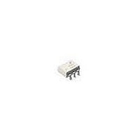
H11N3SR2VM Fairchild Semiconductor, H11N3SR2VM Datasheet - Page 2

H11N3SR2VM
Manufacturer Part Number
H11N3SR2VM
Description
High Speed Optocouplers Optocoupler LC Schmitt Trigger
Manufacturer
Fairchild Semiconductor
Specifications of H11N3SR2VM
Isolation Voltage
5300 Vrms
Maximum Continuous Output Current
50 mA
Maximum Fall Time
12 ns
Maximum Forward Diode Current
30 mA
Maximum Rise Time
7.5 ns
Output Device
Logic Gate Photo IC
Configuration
1 Channel
Maximum Baud Rate
5 MBps
Maximum Forward Diode Voltage
2 V
Maximum Reverse Diode Voltage
6 V
Maximum Power Dissipation
250 mW
Maximum Operating Temperature
+ 85 C
Minimum Operating Temperature
- 40 C
Package / Case
SMD-6
Number Of Elements
1
Input Type
DC
Output Type
Open Collector
Forward Voltage
2V
Forward Current
30mA
Output Current
50mA
Package Type
PDIP W SMD
Operating Temp Range
-40C to 85C
Power Dissipation
250mW
Propagation Delay Time
330ns
Pin Count
6
Mounting
Surface Mount
Reverse Breakdown Voltage
6V
Operating Temperature Classification
Industrial
Lead Free Status / RoHS Status
Lead free / RoHS Compliant
© 2005 Fairchild Semiconductor Corporation
*Typical values at T
ABSOLUTE MAXIMUM RATINGS
Parameters
TOTAL DEVICE
Storage Temperature
Operating Temperature
Lead Solder Temperature
Total Device Power Dissipation @ 25°C
EMITTER
Continuous Forward Current
Reverse Voltage
Forward Current - Peak (1 µs pulse, 300 pps)
LED Power Dissipation 25°C Ambient
DETECTOR
Detector Power Dissipation @ 25°C
V
V
I
ELECTRICAL CHARACTERISTICS
INDIVIDUAL COMPONENT CHARACTERISTICS
Parameters
EMITTER
Input Forward Voltage
Reverse Current
Capacitance
DETECTOR
Operating Voltage Range
Supply Current
Output Current, High
4
H11N1-M
45
65
Output Current
Derate Above 25°C
Derate Linearly From 25°C
Derate Linearly from 25°C
Allowed Range
Allowed Range
A
= 25°C
I
I
V
V = 0, f = 1.0 MHz
I
I
F
F
F
F
R
= 10 mA
= 0.3 mA
= 0, V
= 0.3mA, V
= 5 V
Test Conditions
CC
= 5V
CC
= V
HIGH SPEED LOGIC OPTOCOUPLERS
O
(T
= 15V
A
= 0-70°C Unless otherwise specified.)
H11N2-M
Page 2 of 9
Symbol
I
CC(off)
V
I
V
C
OH
I
CC
R
F
J
Symbol
I
T
T
T
F
V
P
V
P
P
OPR
V
STG
SOL
(pk)
I
I
CC
O
F
O
D
R
D
D
Device
All
All
All
All
All
All
Device
All
All
All
All
All
All
All
All
All
All
All
All
0.75
Min
4
260 for 10 sec
-55 to +150
Typ*
1.25
-40 to +85
1.4
6
0 to 16
0 to 16
Value
2.94
1.41
1.76
250
120
150
1.0
30
50
6
6-PIN DIP
Max
100
100
10
15
10
H11N3-M
2
mW/°C
mW/°C
mW/°C
Units
mW
mW
mW
mA
mA
°C
°C
°C
V
A
V
V
Units
6/15/05
mA
µA
pF
µA
V
V


