JN5139/001,531 NXP Semiconductors, JN5139/001,531 Datasheet - Page 69
JN5139/001,531
Manufacturer Part Number
JN5139/001,531
Description
MCU 802.15.4 32BIT 2.4G 56-QFN
Manufacturer
NXP Semiconductors
Datasheet
1.JN5139-Z01-V.pdf
(82 pages)
Specifications of JN5139/001,531
Frequency
2.4GHz
Modulation Or Protocol
802.15.4
Applications
General Purpose
Power - Output
*
Sensitivity
-96dBm
Voltage - Supply
2.7 V ~ 3.6 V
Current - Receiving
37mA
Current - Transmitting
37mA
Data Interface
PCB, Surface Mount
Memory Size
96kB RAM, 192kB ROM
Antenna Connector
PCB, Surface Mount
Operating Temperature
-20°C ~ 70°C
Package / Case
56-VFQFN
Core
RISC
Lead Free Status / RoHS Status
Lead free / RoHS Compliant


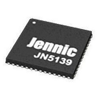
A.4 Device Package Marking
The diagram below shows the package markings for JN5139 devices. The package on the left along with the legend
information below it, shows the general format of package marking. The package on the right shows the specific
markings for a JN5139-001 device, that came from assembly build number 1000004 and was manufactured week 4
of 2007.
Legend:
Where this Data Sheet is denoted as “Advanced” or “Preliminary”, devices will be either Engineering or Prototype
Samples. Devices of this status have an R suffix after the software ROM identifier, for example JN5139-001R.
Devices may also have an additional digit immediately after the R suffix, for example R1, R2, R3 etc. This additional
digit is use to identify different revisions of engineering or prototype silicon during these product phases.
© NXP Laboratories UK 2010
JN XXXX -SSS
JN
XXXX
SSS
FFFFFFF
YY
WW
Jennic
FFFFFFF
YYWW
Jennic
4 digit part number, for example 5139
3 digit software ROM identifier
7 digit assembly build number
2 digit year number
2 digit week number
JN-DS-JN5139 1v9
JN5139-001
Jennic
1000004
0704
69
Related parts for JN5139/001,531
Image
Part Number
Description
Manufacturer
Datasheet
Request
R

Part Number:
Description:
JN5139-Z01-M/SOM041/REEL13 DP
Manufacturer:
NXP Semiconductors
Datasheet:

Part Number:
Description:
JN5139-Z01-M/SOM041/REEL PACK/
Manufacturer:
NXP Semiconductors
Datasheet:

Part Number:
Description:
JN5139-001-M/SOM041/REEL13 DP
Manufacturer:
NXP Semiconductors
Datasheet:

Part Number:
Description:
JN5139-Z01-M/SOM041/REEL13 DP
Manufacturer:
NXP Semiconductors
Datasheet:

Part Number:
Description:
JN5139-Z01-M/SOM041/REEL PACK/
Manufacturer:
NXP Semiconductors
Datasheet:

Part Number:
Description:
JN5139-001-M/SOM041/REEL PACK/
Manufacturer:
NXP Semiconductors
Datasheet:

Part Number:
Description:
JN5139-001-M/SOM041/REEL PACK/
Manufacturer:
NXP Semiconductors
Datasheet:

Part Number:
Description:
JN5139-001-M/SOM041/REEL13 DP
Manufacturer:
NXP Semiconductors
Datasheet:

Part Number:
Description:
JN5139-Z01-M/SOM041/REEL13 DP
Manufacturer:
NXP Semiconductors
Datasheet:
Part Number:
Description:
JN5139-001-M/SOM041/REEL13 DP
Manufacturer:
NXP Semiconductors
Datasheet:

Part Number:
Description:
IC MCU ZIGBEE 32BIT 2.4G 56QFN
Manufacturer:
NXP Semiconductors
Datasheet:
Part Number:
Description:
IC MCU 802.15.4 32BIT 2.4G 56QFN
Manufacturer:
NXP Semiconductors
Datasheet:

Part Number:
Description:
KIT EVAL IEEE802.15.4 JN5139
Manufacturer:
Jennic LTD
Datasheet:

Part Number:
Description:
ZigBee Module W/ Integrated Antenna
Manufacturer:
Jennic LTD
Datasheet:

Part Number:
Description:
32BIT MCU, ZIGBEE, 192K ROM, 5139
Manufacturer:
Jennic LTD
Datasheet: