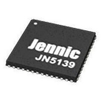
JN5139/001,531 NXP Semiconductors, JN5139/001,531 Datasheet - Page 60

JN5139/001,531
Manufacturer Part Number
JN5139/001,531
Description
MCU 802.15.4 32BIT 2.4G 56-QFN
Manufacturer
NXP Semiconductors
Datasheet
1.JN5139-Z01-V.pdf
(82 pages)
Specifications of JN5139/001,531
Frequency
2.4GHz
Modulation Or Protocol
802.15.4
Applications
General Purpose
Power - Output
*
Sensitivity
-96dBm
Voltage - Supply
2.7 V ~ 3.6 V
Current - Receiving
37mA
Current - Transmitting
37mA
Data Interface
PCB, Surface Mount
Memory Size
96kB RAM, 192kB ROM
Antenna Connector
PCB, Surface Mount
Operating Temperature
-20°C ~ 70°C
Package / Case
56-VFQFN
Core
RISC
Lead Free Status / RoHS Status
Lead free / RoHS Compliant
- Current page: 60 of 82
- Download datasheet (619Kb)
17.3.10
VDD = 3.0V, VREF = 1.2V, -40 to +85ºC
60
Resolution
Current consumption
Integral nonlinearity
Differential nonlinearity
Offset error
Gain error
Internal clock
Output settling time to
0.5LSB
Minimum Update time
Output voltage swing
Output voltage swing
Vref (Internal)
VREF (External)
Resistive load
Capacitive load
Digital input coding
Parameter
Digital to Analogue Converters
Min
0.8
10
10
-1
0
0
2x(Vdd-1.2 )
Vdd-1.2 and
and Vdd-0.2
215 (single)
and 2xVref
235 (both)
JN-DS-JN5139 1v9
Lower of
Lower of
500kHz,
250kHz
2MHz,
1MHz,
Binary
Typ
Vref
±10
±10
1.2
11
±2
5
See Section 17.3.8 Bandgap Reference
Max
1.6
+1
20
Unit
LSB
LSB
bits
mV
mV
µA
kΩ
µs
µs
pF
V
V
V
© NXP Laboratories UK 2010
Guaranteed monotonic
16MHz input clock,
programmable
prescaler
With 10k ohms & 20pF
load
2MHz Clock with
sample period of 8
Output voltage swing
Gain =0
Output voltage swing
Gain =1
Allowable range into
VREF pin
To ground
Notes
Related parts for JN5139/001,531
Image
Part Number
Description
Manufacturer
Datasheet
Request
R

Part Number:
Description:
JN5139-Z01-M/SOM041/REEL13 DP
Manufacturer:
NXP Semiconductors
Datasheet:

Part Number:
Description:
JN5139-Z01-M/SOM041/REEL PACK/
Manufacturer:
NXP Semiconductors
Datasheet:

Part Number:
Description:
JN5139-001-M/SOM041/REEL13 DP
Manufacturer:
NXP Semiconductors
Datasheet:

Part Number:
Description:
JN5139-Z01-M/SOM041/REEL13 DP
Manufacturer:
NXP Semiconductors
Datasheet:

Part Number:
Description:
JN5139-Z01-M/SOM041/REEL PACK/
Manufacturer:
NXP Semiconductors
Datasheet:

Part Number:
Description:
JN5139-001-M/SOM041/REEL PACK/
Manufacturer:
NXP Semiconductors
Datasheet:

Part Number:
Description:
JN5139-001-M/SOM041/REEL PACK/
Manufacturer:
NXP Semiconductors
Datasheet:

Part Number:
Description:
JN5139-001-M/SOM041/REEL13 DP
Manufacturer:
NXP Semiconductors
Datasheet:

Part Number:
Description:
JN5139-Z01-M/SOM041/REEL13 DP
Manufacturer:
NXP Semiconductors
Datasheet:

Part Number:
Description:
JN5139-001-M/SOM041/REEL13 DP
Manufacturer:
NXP Semiconductors
Datasheet:

Part Number:
Description:
IC MCU ZIGBEE 32BIT 2.4G 56QFN
Manufacturer:
NXP Semiconductors
Datasheet:

Part Number:
Description:
IC MCU 802.15.4 32BIT 2.4G 56QFN
Manufacturer:
NXP Semiconductors
Datasheet:

Part Number:
Description:
KIT EVAL IEEE802.15.4 JN5139
Manufacturer:
Jennic LTD
Datasheet:

Part Number:
Description:
ZigBee Module W/ Integrated Antenna
Manufacturer:
Jennic LTD
Datasheet:

Part Number:
Description:
32BIT MCU, ZIGBEE, 192K ROM, 5139
Manufacturer:
Jennic LTD
Datasheet:


