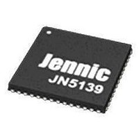
JN5139/001,531 NXP Semiconductors, JN5139/001,531 Datasheet - Page 16

JN5139/001,531
Manufacturer Part Number
JN5139/001,531
Description
MCU 802.15.4 32BIT 2.4G 56-QFN
Manufacturer
NXP Semiconductors
Datasheet
1.JN5139-Z01-V.pdf
(82 pages)
Specifications of JN5139/001,531
Frequency
2.4GHz
Modulation Or Protocol
802.15.4
Applications
General Purpose
Power - Output
*
Sensitivity
-96dBm
Voltage - Supply
2.7 V ~ 3.6 V
Current - Receiving
37mA
Current - Transmitting
37mA
Data Interface
PCB, Surface Mount
Memory Size
96kB RAM, 192kB ROM
Antenna Connector
PCB, Surface Mount
Operating Temperature
-20°C ~ 70°C
Package / Case
56-VFQFN
Core
RISC
Lead Free Status / RoHS Status
Lead free / RoHS Compliant
- Current page: 16 of 82
- Download datasheet (619Kb)
When bootloading program code from external serial memory, the JN5139 automatically accesses the encryption key
to execute the decryption process. User program code does not need to handle any of the decryption process; it is a
transparent process.
With encryption enabled, the time taken to boot code from external Flash memory is increased.
4.5 Peripherals
All peripherals have their registers mapped into the memory space. Access to these registers requires 3 clock
cycles. Applications have access to the peripherals through the software libraries that present a high-level view of
the peripheral’s functions through a series of dedicated software routines. These routines provide both a tested
method for using the peripherals and allow bug-free application code to be developed more rapidly. For details, see
the Integrated Peripherals API Reference Manual (JN-RM-2001).
4.6 Unused Memory Addresses
Any attempt to access an unpopulated memory area will result in a bus error exception (interrupt) being generated.
16
JN-DS-JN5139 1v9
© NXP Laboratories UK 2010
Related parts for JN5139/001,531
Image
Part Number
Description
Manufacturer
Datasheet
Request
R

Part Number:
Description:
JN5139-Z01-M/SOM041/REEL13 DP
Manufacturer:
NXP Semiconductors
Datasheet:

Part Number:
Description:
JN5139-Z01-M/SOM041/REEL PACK/
Manufacturer:
NXP Semiconductors
Datasheet:

Part Number:
Description:
JN5139-001-M/SOM041/REEL13 DP
Manufacturer:
NXP Semiconductors
Datasheet:

Part Number:
Description:
JN5139-Z01-M/SOM041/REEL13 DP
Manufacturer:
NXP Semiconductors
Datasheet:

Part Number:
Description:
JN5139-Z01-M/SOM041/REEL PACK/
Manufacturer:
NXP Semiconductors
Datasheet:

Part Number:
Description:
JN5139-001-M/SOM041/REEL PACK/
Manufacturer:
NXP Semiconductors
Datasheet:

Part Number:
Description:
JN5139-001-M/SOM041/REEL PACK/
Manufacturer:
NXP Semiconductors
Datasheet:

Part Number:
Description:
JN5139-001-M/SOM041/REEL13 DP
Manufacturer:
NXP Semiconductors
Datasheet:

Part Number:
Description:
JN5139-Z01-M/SOM041/REEL13 DP
Manufacturer:
NXP Semiconductors
Datasheet:

Part Number:
Description:
JN5139-001-M/SOM041/REEL13 DP
Manufacturer:
NXP Semiconductors
Datasheet:

Part Number:
Description:
IC MCU ZIGBEE 32BIT 2.4G 56QFN
Manufacturer:
NXP Semiconductors
Datasheet:

Part Number:
Description:
IC MCU 802.15.4 32BIT 2.4G 56QFN
Manufacturer:
NXP Semiconductors
Datasheet:

Part Number:
Description:
KIT EVAL IEEE802.15.4 JN5139
Manufacturer:
Jennic LTD
Datasheet:

Part Number:
Description:
ZigBee Module W/ Integrated Antenna
Manufacturer:
Jennic LTD
Datasheet:

Part Number:
Description:
32BIT MCU, ZIGBEE, 192K ROM, 5139
Manufacturer:
Jennic LTD
Datasheet:


