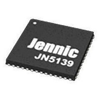
JN5139/001,531 NXP Semiconductors, JN5139/001,531 Datasheet - Page 17

JN5139/001,531
Manufacturer Part Number
JN5139/001,531
Description
MCU 802.15.4 32BIT 2.4G 56-QFN
Manufacturer
NXP Semiconductors
Datasheet
1.JN5139-Z01-V.pdf
(82 pages)
Specifications of JN5139/001,531
Frequency
2.4GHz
Modulation Or Protocol
802.15.4
Applications
General Purpose
Power - Output
*
Sensitivity
-96dBm
Voltage - Supply
2.7 V ~ 3.6 V
Current - Receiving
37mA
Current - Transmitting
37mA
Data Interface
PCB, Surface Mount
Memory Size
96kB RAM, 192kB ROM
Antenna Connector
PCB, Surface Mount
Operating Temperature
-20°C ~ 70°C
Package / Case
56-VFQFN
Core
RISC
Lead Free Status / RoHS Status
Lead free / RoHS Compliant
5 System Clocks
Two system clocks are used to provide timing references into the on-chip subsystems of the JN5139. A 16MHz clock,
generated by a crystal-controlled 16MHz oscillator, is used by the transceiver, processor, memory and digital and
analogue peripherals. A 32kHz clock is used by the sleep timer and during the startup phase of the chip.
5.1 16MHz System Clock / Crystal Oscillator
The JN5139 contains the necessary on-chip components to build a 16 MHz reference oscillator with the addition of
an external crystal resonator, two tuning capacitors and a resistor. The schematic of these components are shown in
Figure 9. The two capacitors, C1 and C2, will typically be 15pF ±5% and use a COG dielectric, R2 should be 1M5Ω.
Due to the small size of the capacitors, it is important to keep the traces to the external components as short as
possible. The on-chip transconductance amplifier is compensated for temperature variation, and is self-biasing by
means of the internal resistor R1. The electrical specification of the oscillator can be found in section 17.3.7. For
detailed application support and specification of the crystal required and factors affecting C1 and C2 see Appendix
B.1.
The clock generated by this oscillator provides the reference for most of the JN5139 subsystems, including the
transceiver, processor, memory and digital and analogue peripherals.
5.2 32kHz System Clock
The 32kHz system clock is used for timing the length of a sleep period (see section 16 Power Management and
Sleep Modes) and also to generate the system clock used internally during reset. The clock can be selected from
one of two sources through the application software:
Once a clock source has been selected, then it will remain in use for all 32kHz timing until a chip reset is performed.
Upon a chip reset the JN5139 defaults to using the internal 32kHz RC Oscillator.
5.2.1 32kHz RC Oscillator
The internal 32kHz RC oscillator is the default clock and requires no external components. It provides a low speed
clock for use in sleep mode. The internal timing components of the oscillator have a wide tolerance due to
manufacturing process variation and so the oscillator runs nominally at 32kHz ±30%. To make this useful as a timing
source for accurate wakeup from sleep, a frequency calibration factor derived from the more accurate 16MHz clock
may be applied. The calibration factor is derived through software, details can be found in section 12.3.1. For detailed
electrical specifications, see section 17.3.6.
© NXP Laboratories UK 2010
•
•
32kHz RC Oscillator
32kHz External Clock
R2
XTALIN
Figure 9: Crystal oscillator connections
C1
JN-DS-JN5139 1v9
R1
C2
XTALOUT
JN5139
17


