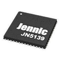
JN5139/001,531 NXP Semiconductors, JN5139/001,531 Datasheet - Page 49

JN5139/001,531
Manufacturer Part Number
JN5139/001,531
Description
MCU 802.15.4 32BIT 2.4G 56-QFN
Manufacturer
NXP Semiconductors
Datasheet
1.JN5139-Z01-V.pdf
(82 pages)
Specifications of JN5139/001,531
Frequency
2.4GHz
Modulation Or Protocol
802.15.4
Applications
General Purpose
Power - Output
*
Sensitivity
-96dBm
Voltage - Supply
2.7 V ~ 3.6 V
Current - Receiving
37mA
Current - Transmitting
37mA
Data Interface
PCB, Surface Mount
Memory Size
96kB RAM, 192kB ROM
Antenna Connector
PCB, Surface Mount
Operating Temperature
-20°C ~ 70°C
Package / Case
56-VFQFN
Core
RISC
Lead Free Status / RoHS Status
Lead free / RoHS Compliant
15.3 Comparators
The JN5139 contains two analogue comparators COMP1 and COMP2 that are designed to have true rail-to-rail
inputs and operate over the full voltage range of the analogue supply VDD1. The hysteresis level (common to both
comparators) can be set to a nominal value of 0mV, 10mV, 20mV or 40mV. In addition, the source of the negative
input signal for each comparator (COMP1M and COMP2M) can be set to the internal voltage reference, the output of
DAC1 or DAC2 (COMP1 or COMP2 respectively) or the appropriate external pin. The comparator outputs are routed
to internal registers and can be polled, or can be used to generate interrupts. The comparators can be disabled to
reduce power consumption.
The comparators have a low power mode where the response time of the comparator is slower than normal and is
specified in section 17.3.11. This mode may be used during non-sleep operation however it is particularly useful in
sleep mode to wake up the JN5139 from sleep where low current consumption is important. The wakeup action and
the configuration for which edge of the comparator output will be active are controlled through software. In sleep
mode the negative input signal source, must be configured to be driven from the external pins.
© NXP Laboratories UK 2010
JN-DS-JN5139 1v9
49


