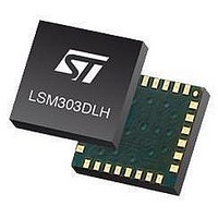
LSM303DLHTR STMicroelectronics, LSM303DLHTR Datasheet - Page 26

LSM303DLHTR
Manufacturer Part Number
LSM303DLHTR
Description
IC ACCELEROMETER 3AXIS 3D 28LGA
Manufacturer
STMicroelectronics
Datasheet
1.STEVAL-MKI063V1.pdf
(47 pages)
Specifications of LSM303DLHTR
Output Type
Digital - I²C
Sensor Type
Accelerometer and Magnetometer
Sensing Axis
Triple
Acceleration
2 g, 4 g, 8 g
Sensitivity
1 mg/digit, 2 mg/digit, 3.9 mg/digit
Package / Case
LGA-28L
Digital Output - Number Of Bits
16 bit
Supply Voltage (max)
3.3 V
Supply Voltage (min)
2.5 V
Maximum Operating Temperature
+ 85 C
Minimum Operating Temperature
- 30 C
Digital Output - Bus Interface
I2C
For Use With
497-10689 - BOARD ADAPTER LSM303DLH DIL24
Lead Free Status / RoHS Status
Lead free / RoHS Compliant
Other names
497-10765-2
LSM303DLHTR
LSM303DLHTR
Available stocks
Company
Part Number
Manufacturer
Quantity
Price
Company:
Part Number:
LSM303DLHTR
Manufacturer:
ST
Quantity:
8 295
Company:
Part Number:
LSM303DLHTR-SMJ
Manufacturer:
ST
Quantity:
8 305
Digital interfaces
26/47
The SCL_M and SDA_M lines in this bus specification can be connected to a host of
devices. The bus can be a single master to multiple slaves, or it can be a multiple master
configuration. All data transfers are initiated by the master device which is responsible for
generating the clock signal, and the data transfers are 8 bits long. All devices are addressed
by the unique 7-bit address of the I
a 9th clock pulse, and releases the SDA_M line.
The receiving device (addressed slave) pulls the SDA_M line low to acknowledge (ACK) the
successful transfer, or leaves the SDA_M high to negative acknowledge (NACK). As per the
I
requirement leads to two unique conditions on the bus associated with the SDA_M
transitions when SCL_M is high. The master device pulling the SDA line low while the
SCL_M line is high indicates the Start (S) condition, while the Stop (P) condition is indicated
by the SDA_M line pulled high while the SCL_M line is high. The I
the Restart condition, in which the master device issues a second start condition without
issuing a stop.
All bus transactions begin with the master device issuing the start sequence followed by the
slave address byte. The address byte contains the slave address; the upper 7 bits (bits7-1),
and the least significant bit (LSb). The LSb of the address byte designates if the operation is
a read (LSb=1) or a write (LSb=0). At the 9th clock pulse, the receiving slave device issues
the ACK (or NACK). Following these bus events, the master sends data bytes for a write
operation, or the slave clocks out data with a read operation. All bus transactions are
terminated with the master issuing a stop sequence.
I
hardware designs release the SDA_M and SCL_M lines as appropriate to allow the slave
device to manipulate these lines. In a software implementation, care must be taken to
perform these tasks in code.
Table 16.
Magnetic signal interface reading/writing
The interface uses an address pointer to indicate which register location is to be read from
or written to. These pointer locations are sent from the master to this slave device and
succeed the 7-bit address plus 1 bit read/write identifier.
To minimize the communication between the master and magnetic digital interface of the
LSM303DLH, the address pointer is updated automatically without master intervention.
This automatic address pointer update has two additional features. First, when address 12
or higher is accessed the pointer updates to address 00, and secondly when address 09 is
reached, the pointer rolls back to address 03. Logically, the address pointer operation
functions as shown below.
●
●
●
●
Any attempt to read an invalid address location returns 0’s, and any write to an invalid
address location or an undefined bit within a valid address location is ignored by this device.
2
2
C specification, all transitions in the SDA_M line must occur when SCL_M is low. This
C bus control can be implemented with either hardware logic or in software. Typical
if address pointer = 09, then address pointer = 03
while if address pointer >12, then address pointer = 0
while address pointer = address pointer + 1
the address pointer value itself cannot be read via the I
Command
Read
Write
SAD+Read/Write patterns
SAD[6:0]
0011110
0011110
Doc ID 16941 Rev 1
2
C. After each 8-bit transfer, the master device generates
R/W
1
0
2
C bus.
00111101 (3Dh)
00111100 (3Ch)
2
C protocol also allows for
SAD+R/W
LSM303DLH


