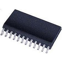
CS5460A-BS Cirrus Logic Inc, CS5460A-BS Datasheet - Page 5

CS5460A-BS
Manufacturer Part Number
CS5460A-BS
Description
Driver IC
Manufacturer
Cirrus Logic Inc
Datasheet
1.CS5460A-BSZ.pdf
(54 pages)
Specifications of CS5460A-BS
Peak Reflow Compatible (260 C)
No
Supply Voltage Max
5V
Driver Case Style
SSOP
Leaded Process Compatible
No
Mounting Type
Surface Mount
Package / Case
24-SSOP
Mounting Style
SMD/SMT
Lead Free Status / RoHS Status
Contains lead / RoHS non-compliant
Available stocks
Company
Part Number
Manufacturer
Quantity
Price
Part Number:
CS5460A-BS
Manufacturer:
CIRRUS
Quantity:
20 000
Company:
Part Number:
CS5460A-BSZ
Manufacturer:
CIRRUS
Quantity:
2
Company:
Part Number:
CS5460A-BSZR
Manufacturer:
CIRRUS
Quantity:
8 000
Part Number:
CS5460A-BSZR
Manufacturer:
CIRRUS
Quantity:
20 000
1. CHARACTERISTICS & SPECIFICATIONS
ANALOG CHARACTERISTICS
(T
K = 1; N = 4000 ==> OWR = 4000 Sps.)(See Notes 1, 2, 3, 4, and 5.)
Notes:
DS487F4
Accuracy (Both Channels)
Common Mode Rejection
Offset Drift (Without the High Pass Filter)
Analog Inputs (Current Channel)
Maximum Differential Input Voltage Range
{(V
Total Harmonic Distortion
Common Mode + Signal on IIN+ or IIN-
Crosstalk with Voltage Channel at Full Scale
Input Capacitance
Effective Input Impedance
Noise (Referred to Input)
Accuracy (Current Channel)
Bipolar Offset Error
Full-Scale Error
Analog Inputs (Voltage Channel)
Maximum Differential Input Voltage Range
Total Harmonic Distortion
Common Mode + Signal on VIN+ or VIN-
Crosstalk with Current Channel at Full Scale
Input Capacitance
Effective Input Impedance
Noise (Referred to Input)
Accuracy (Voltage Channel)
Bipolar Offset Error
Full-Scale Error
A
IIN+
= -40 °C to +85 °C; VA+ = VD+ = +5 V ±10%; VREFIN = +2.5 V; VA- = AGND = 0 V; MCLK = 4.096 MHz,
) - (V
1. Bipolar Offset Errors and Full-Scale Gain Errors for the current and voltage channels refer to the respective Irms
2. Specifications guaranteed by design, characterization, and/or test.
3. Analog signals are relative to VA- and digital signals to DGND unless otherwise noted.
4. In requiring VA+ = VD+ =5 V ±10%, note that it is allowable for VA+, VD+ to differ by as much as ±200 mV, as long
5. Note that “Sps” is an abbreviation for units of “samples per second”.
6. Effective Input Impedance (Zin) is determined by clock frequency (DCLK) and Input Capacitance (IC).
IIN-
Register and Vrms Register output, when the device is operating in ‘continuous computation cycles’ data acquisition
mode, after offset/gain system calibration sequences have been executed. These specs do not apply to the error
of the Instantaneous Current/Voltage Register output.
as VA+ > VD+.
Zin = 1/(IC*DCLK/4). Note that DCLK = MCLK / K.
)}
Parameter
(Gain = 10 or 50)
{(V
(DC, 50, 60 Hz)
VIN+
(Gain = 10)
(Gain = 50)
(Gain = 10)
(Gain = 50)
(Gain = 10)
(Gain = 50)
(Gain = 10)
(Gain = 50)
(50, 60 Hz)
(50, 60 Hz)
) - (V
(Note 6)
(Note 1)
(Note 1)
(Note 6)
(Note 1)
(Note 1)
VIN-
)}
Symbol
CMRR
THD
VOS
FSE
THD
VOS
FSE
C
Z
V
C
Z
Z
I
IN
inV
inV
inI
inI
IN
in
V
V
V
I
I
I
-0.25
Min
VA-
80
80
62
-
-
-
-
-
-
-
-
-
-
-
-
-
-
-
-
-
-
-
±0.001
±0.001
±0.01
±0.01
Typ
0.2
25
25
30
30
5
5
-
-
-
-
-
-
-
-
-
-
-
-
-
Max
VA+
-115
VA+
500
100
500
250
CS5460A
-70
20
4
-
-
-
-
-
-
-
-
-
-
-
-
-
-
mV
mV
mV
nV/°C
%F.S.
%F.S.
%F.S.
%F.S.
µV
µV
µV
Unit
MΩ
kΩ
kΩ
dB
dB
dB
pF
pF
dB
dB
pF
V
V
rms
rms
rms
P-P
P-P
P-P
5


