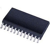
CS5460A-BS Cirrus Logic Inc, CS5460A-BS Datasheet - Page 46

CS5460A-BS
Manufacturer Part Number
CS5460A-BS
Description
Driver IC
Manufacturer
Cirrus Logic Inc
Datasheet
1.CS5460A-BSZ.pdf
(54 pages)
Specifications of CS5460A-BS
Peak Reflow Compatible (260 C)
No
Supply Voltage Max
5V
Driver Case Style
SSOP
Leaded Process Compatible
No
Mounting Type
Surface Mount
Package / Case
24-SSOP
Mounting Style
SMD/SMT
Lead Free Status / RoHS Status
Contains lead / RoHS non-compliant
Available stocks
Company
Part Number
Manufacturer
Quantity
Price
Part Number:
CS5460A-BS
Manufacturer:
CIRRUS
Quantity:
20 000
Company:
Part Number:
CS5460A-BSZ
Manufacturer:
CIRRUS
Quantity:
2
Company:
Part Number:
CS5460A-BSZR
Manufacturer:
CIRRUS
Quantity:
8 000
Part Number:
CS5460A-BSZR
Manufacturer:
CIRRUS
Quantity:
20 000
5.2 Current Channel DC Offset Register and Voltage Channel DC Offset Register
5.3 Current Channel Gain Register and Voltage Channel Gain Register
5.4 Cycle Count Register
46
MSB
MSB
MSB
-(2
2
2
23
1
0
Address:
Default** = 0.000
The DC offset registers are initialized to zero on reset, allowing the device to function and perform measure-
ments. The register is loaded after one computation cycle with the current or voltage offset when the proper input
is applied and the DC Calibration Command is received. DRDY will be asserted at the end of the calibration.
The register may be read and stored so the register may be restored with the desired system offset compensa-
tion. The value is in the range ± full scale. The numeric format of this register is two’s complement notation.
Address:
Default** = 1.000
The gain registers are initialized to 1.0 on reset, allowing the device to function and perform measurements. The
gain registers hold the result of either the AC or DC gain calibrations, whichever was most recently performed.
If DC calibration is performed, the register is loaded after one computation cycle with the system gain when the
proper DC input is applied and the Calibration Command is received. If AC calibration is performed, then after
~(6N + 30) A/D conversion cycles (where N is the value of the Cycle-Count Register) the register(s) is loaded
with the system gain when the proper AC input is applied and the Calibration Command is received. DRDY will
be asserted at the end of the calibration. The register may be read and stored so the register may be restored
with the desired system offset compensation. The value is in the range 0.0 ≤ Gain < 4.0.
Address: 5
Default** = 4000
The Cycle Count Register value (denoted as ‘N’) specifies the number of A/D conversion cycles per computation
cycle. For each computation cycle, the updated results in the RMS and Energy Registers are computed using
the most recent set of N continuous instantaneous voltage/current samples. When the device is commanded to
operate in ’continuous computation cycles’ data acquisition mode, the computation cycle frequency is
(MCLK / K) / (1024 ∗ N) where MCLK is master clock input frequency (into XIN / XOUT pins), K is the clock di-
vider value (as specified in the Configuration Register), and N is Cycle Count Register value.
)
2
2
2
22
-1
0
1 (Current Channel DC Offset Register)
3 (Voltage Channel DC Offset Register)
2 (Current Channel Gain Register)
4 (Voltage Channel Gain Register)
2
2
2
21
-2
-1
2
2
2
20
-3
-2
2
2
2
19
-4
-3
2
2
2
18
-5
-4
2
2
2
17
-6
-5
2
2
2
16
-7
-6
.....
.....
.....
2
2
2
-17
-16
6
2
2
2
-18
-17
5
2
2
2
-19
-18
4
2
2
2
-20
-19
3
2
2
2
-21
-20
2
CS5460A
2
2
2
-22
-21
1
DS487F4
LSB
LSB
LSB
2
2
2
-23
-22
0


