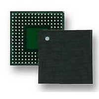
LH7A404N0F000B3 NXP Semiconductors, LH7A404N0F000B3 Datasheet - Page 48

LH7A404N0F000B3
Manufacturer Part Number
LH7A404N0F000B3
Description
MCU ARM9, LCD CTRL, SMD, LFBGA-324
Manufacturer
NXP Semiconductors
Datasheet
1.LH7A404N0F000B3.pdf
(75 pages)
Specifications of LH7A404N0F000B3
Core Size
32bit
No. Of I/o's
64
Ram Memory Size
80KB
Cpu Speed
200MHz
Oscillator Type
External Only
No. Of Timers
3
No. Of Pwm Channels
4
Digital Ic Case Style
LFBGA
Supply Voltage Range
3V
Controller Family/series
LH7A
Peripherals
ADC, DMA, RTC
Rohs Compliant
Yes
Data Bus Width
32 bit
Program Memory Type
ROMLess
Data Ram Size
80 KB
Interface Type
EBI , IrDA , JTAG , PS2 , SCI , UART , USB
Maximum Clock Frequency
200 MHz
Number Of Programmable I/os
64
Number Of Timers
3
Maximum Operating Temperature
+ 85 C
Mounting Style
SMD/SMT
Package / Case
LFBGA
Minimum Operating Temperature
- 40 C
On-chip Adc
10 bit, 9 Channel
Lead Free Status / RoHS Status
Lead free / RoHS Compliant
Available stocks
Company
Part Number
Manufacturer
Quantity
Price
Company:
Part Number:
LH7A404N0F000B3
Manufacturer:
AD
Quantity:
5 742
Company:
Part Number:
LH7A404N0F000B3,55
Manufacturer:
NXP Semiconductors
Quantity:
10 000
LH7A404
SSP Waveforms
data frame formats:
• Texas Instruments SSI
• Motorola SPI
• National Semiconductor MICROWIRE
length, depending upon the programmed data size.
Each data frame is transmitted beginning with the
Most Significant Bit (MSB) i.e. ‘big endian’. For all
three formats, the SSP serial clock is held LOW (inac-
tive) while the SSP is idle. The SSP serial clock tran-
sitions only during active transmission of data. The
48
The Synchronous Serial Port (SSP) supports three
Each frame format is between 4 and 16 bits in
Figure 21. Texas Instruments Synchronous Serial Frame Format (Continuous Transfer)
Figure 20. Texas Instruments Synchronous Serial Frame Format (Single Transfer)
SSPTXD/
SSPTXD/
SSPFRM
SSPFRM
SSPRXD
SSPRXD
SSPCLK
SSPCLK
MSB
MSB
NXP Semiconductors
4 to 16 BITS
4 to 16 BITS
SSPFRM signal marks the beginning and end of a
frame.
synchronous serial frame format, Figure 22 through
Figure 29 show the Motorola SPI format, and Figure 30
and Figure 31 show National Semiconductor’s MICRO-
WIRE data frame format.
is pulsed prior to each frame’s transmission for one
serial clock period beginning at its rising edge. For this
frame format, both the SSP and the external slave
device drive their output data on the rising edge of the
clock and latch data from the other device on the falling
edge. See Figure 20 and Figure 21.
Figure 20 and Figure 21 show Texas Instruments
For Texas Instruments SSI format, the SSPFRM pin
LSB
LSB
32-Bit System-on-Chip
Preliminary data sheet
LH7A404-24
LH7A404-25


