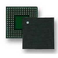
LH7A404N0F000B3 NXP Semiconductors, LH7A404N0F000B3 Datasheet - Page 18

LH7A404N0F000B3
Manufacturer Part Number
LH7A404N0F000B3
Description
MCU ARM9, LCD CTRL, SMD, LFBGA-324
Manufacturer
NXP Semiconductors
Datasheet
1.LH7A404N0F000B3.pdf
(75 pages)
Specifications of LH7A404N0F000B3
Core Size
32bit
No. Of I/o's
64
Ram Memory Size
80KB
Cpu Speed
200MHz
Oscillator Type
External Only
No. Of Timers
3
No. Of Pwm Channels
4
Digital Ic Case Style
LFBGA
Supply Voltage Range
3V
Controller Family/series
LH7A
Peripherals
ADC, DMA, RTC
Rohs Compliant
Yes
Data Bus Width
32 bit
Program Memory Type
ROMLess
Data Ram Size
80 KB
Interface Type
EBI , IrDA , JTAG , PS2 , SCI , UART , USB
Maximum Clock Frequency
200 MHz
Number Of Programmable I/os
64
Number Of Timers
3
Maximum Operating Temperature
+ 85 C
Mounting Style
SMD/SMT
Package / Case
LFBGA
Minimum Operating Temperature
- 40 C
On-chip Adc
10 bit, 9 Channel
Lead Free Status / RoHS Status
Lead free / RoHS Compliant
Available stocks
Company
Part Number
Manufacturer
Quantity
Price
Company:
Part Number:
LH7A404N0F000B3
Manufacturer:
AD
Quantity:
5 742
Company:
Part Number:
LH7A404N0F000B3,55
Manufacturer:
NXP Semiconductors
Quantity:
10 000
LH7A404
SYSTEM DESCRIPTIONS
ARM922T Processor
cached core with an Advanced High-performance Bus
(AHB) interface. The processor is a member of the
ARM9T family of processors. For more information, see
the ARM document, ‘ARM922T Technical Reference
Manual’, available on ARM’s website at www.arm.com.
Clock and State Controller
around two primary oscillator inputs. These are the
14.7456 MHz input crystal and the 32.768 kHz real time
clock oscillator; see Figure 3. The 14.7456 MHz oscil-
lator supplies the main system clock domains for the
LH7A404. The 32.768 kHz oscillator controls the
power-down operations and real time clock peripheral.
The clock and state controller provides the clock gating
and frequency division necessary, and then supplies
the clocks to the processor and rest of the system. The
amount of clock gating that actually takes place
depends on the power saving mode selected.
18
The LH7A404 microcontroller features the ARM922T
The clocking scheme in the LH7A404 is based
COMPACT
FLASH
CARD
PC
FLASH
SDRAM
ROM
SRAM
PCMCIA
DEVICE
HOST
1
4
7
*
2
5
8
0
GPIO
3
6
9
#
Figure 2. Application Diagram
NXP Semiconductors
LH7A404
USB
HOST
STN/TFT/
AD-TFT
Real Time Clock tree and power-down logic. This clock
is used for the power state control and is the only clock
in the LH7A404 that runs continuously. The 32.768 kHz
clock is divided down to 1 Hz for the Real Time Clock
counter using a ripple divider to save power.
main system clocks for the LH7A404. It is the source
for PLL1 and PLL2, the primary clock for the peripher-
als, and the source clock to the programmable clock
(PGM) divider.
erates the following clocks: FCLK, HCLK, and PCLK.
FCLK is the clock that drives the ARM922T core.
all memory interfaces, bus arbitrators and the AHB
peripherals. HCLK is generated by dividing FCLK by 1,
2, 3, or 4. HCLK can be gated by the system to enable
low power operation.
ated by dividing HCLK by either 2, 4, or 8.
USB peripheral.
IR
The 32.768 kHz clock provides the source for the
The 14.7456 MHz source is used to generate the
PLL1 provides the main clock tree for the chip. It gen-
HCLK is the main bus (AHB) clock, as such it clocks
PCLK is the peripheral bus (APB) clock. It is gener-
PLL2 generates a fixed 48 MHz clock signal for the
UART
SSP
SCREEN
CONTR.
BMI
TOUCH
BATTERY
SCI
SMART
CARD
MMC/SD
DMA
AC97
DC to DC
GENERATION
CODEC
CIRCUITRY
32-Bit System-on-Chip
Preliminary data sheet
VOLTAGE
MULTIMEDIA
CARD
LH7A404-2


