LSM303DLH STMicroelectronics, LSM303DLH Datasheet - Page 33
LSM303DLH
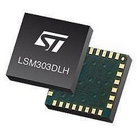
Manufacturer Part Number
LSM303DLH
Description
IC, DIGITAL COMPASS, ±2g ±4g ±8g, LGA-28
Manufacturer
STMicroelectronics
Series
-r
Specifications of LSM303DLH
No. Of Axes
3
Ic Interface Type
I2C, Serial
Sensor Case Style
LGA
No. Of Pins
28
Supply Voltage Range
2.5V To 3.3V
Acceleration Range
± 2g, ± 4g, ± 8g
Sensing Axis
Triple
Acceleration
2 g, 4 g, 8 g
Sensitivity
1 mg/digit, 2 mg/digit, 3.9 mg/digit
Package / Case
LGA-28L
Output Type
Linear
Digital Output - Number Of Bits
16 bit
Supply Voltage (max)
3.3 V
Supply Voltage (min)
2.5 V
Maximum Operating Temperature
+ 85 C
Minimum Operating Temperature
- 30 C
Digital Output - Bus Interface
I2C
Package Type
LGA
Operating Supply Voltage (min)
2.5V
Operating Temperature (max)
85C
Operating Temperature Classification
Commercial
Product Depth (mm)
5mm
Product Height (mm)
1mm
Product Length (mm)
5mm
Mounting
Surface Mount
Pin Count
28
Sensor Type
Accelerometer and Magnetometer
Lead Free Status / Rohs Status
Lead free / RoHS Compliant
For Use With
497-10689 - BOARD ADAPTER LSM303DLH DIL24497-10508 - BOARD EVAL FOR MEMS SENSORS
Available stocks
Company
Part Number
Manufacturer
Quantity
Price

Part Number:
LSM303DLH
Manufacturer:
ST
Quantity:
20 000
Part Number:
LSM303DLHC
Manufacturer:
ST
Quantity:
20 000
Company:
Part Number:
LSM303DLHCTR
Manufacturer:
ST
Quantity:
12 000
Part Number:
LSM303DLHCTR
Manufacturer:
ST
Quantity:
20 000
Company:
Part Number:
LSM303DLHTR
Manufacturer:
ST
Quantity:
8 295
Company:
Part Number:
LSM303DLHTR-SMJ
Manufacturer:
ST
Quantity:
8 305


LSM303DLH
9.1.5
9.1.6
9.1.7
The BDU bit is used to inhibit output register updates between the reading of the upper and
lower register parts. In default mode (BDU = ‘0’), the lower and upper register parts are
updated continuously. If it is not certain to read faster than output data rate, it is
recommended to set BDU bit to ‘1’. In this way, after the reading of the lower (upper) register
part, the content of that output register is not updated until the upper (lower) part is read
also. This feature avoids reading LSB and MSB related to different samples.
CTRL_REG5_A (24h)
Table 31.
Table 32.
TurnOn bits are used for turning on the sleep-to-wake function.
Table 33.
By setting the TurnOn [1:0] bits to 11, the “sleep-to-wake” function is enabled. When an
interrupt event occurs, the device goes into normal mode, increasing the ODR to the value
defined in CTRL_REG1_A. Although the device is in normal mode, CTRL_REG1_A content
is not automatically changed to “normal mode” configuration.
HP_FILTER_RESET_A (25h)
Dummy register. Reading at this address instantaneously zeroes the content of the internal
high-pass filter. If the high-pass filter is enabled, all three axes are instantaneously set to 0
g. This makes it possible to surmount the settling time of the high-pass filter.
REFERENCE_A (26h)
Table 34.
Table 35.
TurnOn1,
TurnOn0
Ref7 - Ref0
TurnOn1
Ref7
0
0
1
CTRL_REG5_A register
CTRL_REG5_A description
Sleep-to-wake configuration
REFERENCE_A register
REFERENCE_A description
Turn-on mode selection for sleep-to-wake function. Default value: 00.
Reference value for high-pass filter. Default value: 00h.
Ref6
0
TurnOn0
0
1
Ref5
0
Sleep-to-wake function is disabled
Turned on: The device is in low-power mode
(ODR is defined in CTRL_REG1_A)
Doc ID 16941 Rev 1
Ref4
0
Sleep-to-wake status
Ref3
0
Ref2
0
Registers description
TurnOn1
Ref1
TurnOn0
Ref0
33/47
Related parts for LSM303DLH
Image
Part Number
Description
Manufacturer
Datasheet
Request
R

Part Number:
Description:
STMicroelectronics [RIPPLE-CARRY BINARY COUNTER/DIVIDERS]
Manufacturer:
STMicroelectronics
Datasheet:
Part Number:
Description:
STMicroelectronics [LIQUID-CRYSTAL DISPLAY DRIVERS]
Manufacturer:
STMicroelectronics
Datasheet:

Part Number:
Description:
BOARD EVAL FOR MEMS SENSORS
Manufacturer:
STMicroelectronics
Datasheet:
Part Number:
Description:
NPN TRANSISTOR POWER MODULE
Manufacturer:
STMicroelectronics
Datasheet:
Part Number:
Description:
TURBOSWITCH ULTRA-FAST HIGH VOLTAGE DIODE
Manufacturer:
STMicroelectronics
Datasheet:
Part Number:
Description:
Manufacturer:
STMicroelectronics
Datasheet:
Part Number:
Description:
DIODE / SCR MODULE
Manufacturer:
STMicroelectronics
Datasheet:
Part Number:
Description:
DIODE / SCR MODULE
Manufacturer:
STMicroelectronics
Datasheet:
Part Number:
Description:
Search -----> STE16N100
Manufacturer:
STMicroelectronics
Datasheet:
Part Number:
Description:
Search ---> STE53NA50
Manufacturer:
STMicroelectronics
Datasheet:
Part Number:
Description:
NPN Transistor Power Module
Manufacturer:
STMicroelectronics
Datasheet:
Part Number:
Description:
DIODE / SCR MODULE
Manufacturer:
STMicroelectronics
Datasheet: