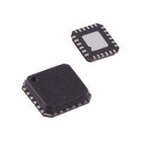
ADL5385ACPZ-R7 Analog Devices Inc, ADL5385ACPZ-R7 Datasheet - Page 3

ADL5385ACPZ-R7
Manufacturer Part Number
ADL5385ACPZ-R7
Description
IC, QUAD MODULATOR 50MHZ-2.2GHZ LFCSP-24
Manufacturer
Analog Devices Inc
Datasheet
1.ADL5385ACPZ-R7.pdf
(24 pages)
Specifications of ADL5385ACPZ-R7
Frequency Range
50MHz To 2.2GHz
Rf Type
Quadrature
Supply Voltage Range
4.75V To 5.5V
Rf Ic Case Style
LFCSP
No. Of Pins
24
Operating Temperature Range
-40°C To +85°C
Design Resources
Broadband Low EVM Direct Conversion Transmitter Using LO Divide-by-2 Modulator (CN0144)
Function
Modulator
Lo Frequency
50MHz ~ 2.2GHz
Rf Frequency
50MHz ~ 2.2GHz
P1db
8dBm
Noise Floor
-160dBm/Hz
Output Power
2.6dBm
Current - Supply
240mA
Voltage - Supply
4.75 V ~ 5.25 V
Test Frequency
2.15GHz
Package / Case
24-VFQFN, 24-CSP Exposed Pad
Rohs Compliant
Yes
Lead Free Status / RoHS Status
Lead free / RoHS Compliant
Other names
ADL5385ACPZ-R7TR
SPECIFICATIONS
Unless otherwise noted, V
bias; baseband frequency = 1 MHz; LO source and RF output load impedances are 50 Ω.
Table 1.
Parameter
OUTPUT FREQUENCY RANGE
EXTERNAL LO FREQUENCY
RANGE
OUTPUT FREQUENCY = 50 MHz
OUTPUT FREQUENCY = 140 MHz
OUTPUT FREQUENCY = 350 MHz
Output Power
Output P1 dB
Carrier Feedthrough
Sideband Suppression
Second Baseband Harmonic
Third Baseband Harmonic
Output IP2
Output IP3
Quadrature Phase Error
I/Q Amplitude Balance
Noise Floor
Output Return Loss
Output Power
Output P1 dB
Carrier Feedthrough
Sideband Suppression
Second Baseband Harmonic
Third Baseband Harmonic
Output IP2
Output IP3
Quadrature Phase Error
I/Q Amplitude Balance
Noise Floor
Output Return Loss
Output Power
Output P1 dB
Carrier Feedthrough
Sideband Suppression
S
= 5 V; T
Single (lower) sideband output
F1 = +3.5 MHz, F2 = +4.5 MHz, P
F1 = +3.5 MHz, F2 = +4.5 MHz, P
Single (lower) sideband output
F1 = +3.5 MHz, F2 = +4.5 MHz, P
F1 = +3.5 MHz, F2 = +4.5 MHz, P
Single (lower) sideband output
Conditions
External LO frequency is twice output frequency
Unadjusted (nominal drive level)
@ +85°C after optimization at +25°C
@ −40°C after optimization at +25°C
Unadjusted (nominal drive level)
@ +85°C after optimization at +25°C
@ −40°C after optimization at +25°C
(F
(F
20 MHz offset from LO, all BB inputs at a bias of 500 mV
20 MHz offset from LO, output power = −5 dBm
Unadjusted (nominal drive level)
@ +85°C after optimization at +25°C
@ −40°C after optimization at +25°C
Unadjusted (nominal drive level)
@ +85°C after optimization at +25°C
@ −40°C after optimization at +25°C
(F
(F
20 MHz offset from LO, all BB inputs at a bias of 500 mV
Unadjusted (nominal drive level)
@ +85°C after optimization at +25°C
@ −40°C after optimization at +25°C
Unadjusted (nominal drive level)
@ +85°C after optimization at +25°C
@ −40°C after optimization at+25°C
A
LO
LO
LO
LO
= 25°C; LO = −7 dBm; I/Q inputs = 1.4 V p-p differential sine waves in quadrature on a 500 mV dc
− (2 × F
+ (3 × F
− (2 × F
+ (3 × F
BB
BB
BB
BB
)), P
)), P
)), P
)), P
OUT
OUT
OUT
OUT
= 5 dBm
= 5 dBm
= 5 dBm
= 5 dBm
Rev. 0 | Page 3 of 24
OUT
OUT
OUT
OUT
= −3 dBm per tone
= −3 dBm per tone
= −3 dBm per tone
=−3 dBm per tone
Min
50
100
4
3
Typ
−0.17
−0.03
−0.33
−0.03
−155
−150
−160
−57
−67
−67
−57
−64
−68
−83
−58
−19
−52
−66
−67
−53
−63
−68
−83
−57
−20
−46
−65
−66
−50
−63
−61
5.6
5.7
5.6
11
69
26
11
70
26
11
Max
2200
4400
8
7
ADL5385
Unit
MHz
MHz
dBm
dBm
dBm
dBm
dBm
dBc
dBc
dBc
dBc
dBc
dBm
dBm
degrees
dB
dBm/Hz
dBm/Hz
dB
dBm
dBm
dBm
dBm
dBm
dBc
dBc
dBc
dBc
dBc
dBm
dBm
degrees
dB
dBm/Hz
dB
dBm
dBm
dBm
dBm
dBm
dBc
dBc
dBc


