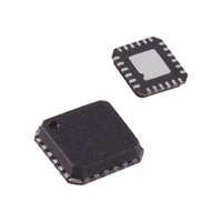
ADL5385ACPZ-R7 Analog Devices Inc, ADL5385ACPZ-R7 Datasheet - Page 13

ADL5385ACPZ-R7
Manufacturer Part Number
ADL5385ACPZ-R7
Description
IC, QUAD MODULATOR 50MHZ-2.2GHZ LFCSP-24
Manufacturer
Analog Devices Inc
Datasheet
1.ADL5385ACPZ-R7.pdf
(24 pages)
Specifications of ADL5385ACPZ-R7
Frequency Range
50MHz To 2.2GHz
Rf Type
Quadrature
Supply Voltage Range
4.75V To 5.5V
Rf Ic Case Style
LFCSP
No. Of Pins
24
Operating Temperature Range
-40°C To +85°C
Design Resources
Broadband Low EVM Direct Conversion Transmitter Using LO Divide-by-2 Modulator (CN0144)
Function
Modulator
Lo Frequency
50MHz ~ 2.2GHz
Rf Frequency
50MHz ~ 2.2GHz
P1db
8dBm
Noise Floor
-160dBm/Hz
Output Power
2.6dBm
Current - Supply
240mA
Voltage - Supply
4.75 V ~ 5.25 V
Test Frequency
2.15GHz
Package / Case
24-VFQFN, 24-CSP Exposed Pad
Rohs Compliant
Yes
Lead Free Status / RoHS Status
Lead free / RoHS Compliant
Other names
ADL5385ACPZ-R7TR
VPOS
BASIC CONNECTIONS
Figure 27 shows the basic connections for the ADL5385.
Power Supply and Grounding
All the VPS pins must be connected to the same 5 V source. Adja-
cent pins of the same name can be tied together and decoupled with
a 0.1 μF capacitor. These capacitors are located as close as possible
to the device. The power supply can range from 4.75 V to 5.5 V.
The COM1 pin, COM2 pin, and COM3 pin are tied to the same
ground plane through low impedance paths. The exposed
paddle on the underside of the package is also soldered to a low
thermal and electrical impedance ground plane. If the ground
plane spans multiple layers on the circuit board, they should be
stitched together with nine vias under the exposed paddle. The
Analog Devices AN-772 application note discusses the thermal
and electrical grounding of the LFCSP in greater detail.
Baseband Inputs
The baseband inputs QBBP, QBBN, IBBP, and IBBN must be
driven from a differential source. The nominal drive level of
1.4 V p-p differential (700 mV p-p on each pin) is biased to
a common-mode level of 500 mV dc.
The dc common-mode bias level for the baseband inputs can
range from 400 mV to 600 mV. This results in a reduction in the
usable input ac swing range. The nominal dc bias of 500 mV
allows for the largest ac swing, limited on the bottom end by the
ADL5385 input range and on the top end by the output
compliance range on most Analog Devices DACs.
LO Input
A single-ended LO signal is applied to the LOIP pin through an
ac coupling capacitor. The recommended LO drive power is
−7 dBm. The LO return pin, LOIN, must be ac-coupled to
ground though a low impedance path.
The nominal LO drive of −7 dBm can be increased to up to
+5 dBm. The effect of LO power on sideband suppression and
carrier feedthrough is shown in Figure 15 and Figure 19.
GND
C11
OPEN
LO
R11
0Ω
CFPQ
OPEN
CLOP
CLON
0.1µF
0.1µF
C12
0.1µF
QBBP
RFPQ
0Ω
Figure 27. Basic Connections for the ADL5385
OPEN
RTQ
19 COM3
20 COM3
21 LOIP
22 LOIN
23 VPS3
24 VPS3
RFNQ
0Ω
QBBN
EXPOSED PADDLE
CFNQ
OPEN
ADL5385
4 × 4 LFCSP
CFNI
OPEN
IBBN
RFNI
0Ω
ENBL 12
VPS2 11
TEMP 10
VPS1 9
VPS1 8
VOUT 7
OPEN
RTI
RFPI
0Ω
IBBP
CFPI
OPEN
ENB
C14
0.1µF
R12
0Ω
C16
0.1µF
RTEMP
200Ω
R13
COUT
0Ω
0.1µF
49.9Ω
R21
C13
OPEN
C15
OPEN
OFF
R22
10kΩ
VPOS
VPOS
TEMP
SW21
ON
VOUT
ENBL
Rev. 0 | Page 13 of 24
RF Output
The RF output is available at the VOUT pin (Pin 7). This pin
must also be ac-coupled. The VOUT pin has a nominal
broadband impedance of 50 Ω and does not need further
external matching.
OPTIMIZATION
The carrier feedthrough and sideband suppression performance
of the ADL5385 can be improved through the use of optimiza-
tion techniques.
Carrier Feedthrough Nulling
Carrier feedthrough results from minute dc offsets that occur
between each of the differential baseband inputs. In an ideal
modulator, the quantities (V
are equal to zero, and this results in no carrier feedthrough. In
a real modulator, those two quantities are nonzero and, when
mixed with the LO, result in a finite amount of carrier feedthrough.
The ADL5385 is designed to provide a minimal amount of carrier
feedthrough. If even lower carrier feedthrough levels are required,
minor adjustments can be made to the (V
V
Q-channel offset is varied until a minimum carrier feedthrough
level is obtained. The Q-channel offset required to achieve this
minimum is held constant while the offset on the I-channel is
adjusted, until a better minimum is reached. Through two
iterations of this process, the carrier feedthrough can be
reduced to as low as the output noise. The ability to null is
sometimes limited by the resolution of the offset adjustment.
Figure 28 shows the relationship of carrier feedthrough vs. dc offset.
Note that throughout the nulling process, the dc bias for the
baseband inputs remains at 500 mV. When no offset is applied,
QOPN
V
V
Figure 28. Carrier Feedthrough vs. DC Offset Voltage at 450 MHz
) offsets. The I-channel offset is held constant while the
IOPP
IOPP
–58
–62
–66
–70
–74
–78
–82
–86
–90
–94
= V
− V
IOPN
IOPN
= 500 mV, or
= V
IOS
= 0 V
VP-VN OFFEST (µV)
IOPP
− V
IOPN
) and (V
IOPP
− V
IOPN
QOPP
) and (V
ADL5385
− V
QOPN
QOPP
)
−


