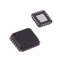
ADL5385ACPZ-R7 Analog Devices Inc, ADL5385ACPZ-R7 Datasheet - Page 12

ADL5385ACPZ-R7
Manufacturer Part Number
ADL5385ACPZ-R7
Description
IC, QUAD MODULATOR 50MHZ-2.2GHZ LFCSP-24
Manufacturer
Analog Devices Inc
Datasheet
1.ADL5385ACPZ-R7.pdf
(24 pages)
Specifications of ADL5385ACPZ-R7
Frequency Range
50MHz To 2.2GHz
Rf Type
Quadrature
Supply Voltage Range
4.75V To 5.5V
Rf Ic Case Style
LFCSP
No. Of Pins
24
Operating Temperature Range
-40°C To +85°C
Design Resources
Broadband Low EVM Direct Conversion Transmitter Using LO Divide-by-2 Modulator (CN0144)
Function
Modulator
Lo Frequency
50MHz ~ 2.2GHz
Rf Frequency
50MHz ~ 2.2GHz
P1db
8dBm
Noise Floor
-160dBm/Hz
Output Power
2.6dBm
Current - Supply
240mA
Voltage - Supply
4.75 V ~ 5.25 V
Test Frequency
2.15GHz
Package / Case
24-VFQFN, 24-CSP Exposed Pad
Rohs Compliant
Yes
Lead Free Status / RoHS Status
Lead free / RoHS Compliant
Other names
ADL5385ACPZ-R7TR
ADL5385
CIRCUIT DESCRIPTION
OVERVIEW
The ADL5385 can be divided into five sections: the local
oscillator (LO) interface, the baseband voltage-to-current (V-to-I)
converter, the mixers, the differential-to-single-ended (D-to-S)
amplifier, and the bias circuit. A detailed block diagram of the
device is shown in Figure 26.
The LO interface generates two LO signals at 90° of phase
difference to drive two mixers in quadrature. Baseband signals
are converted into currents by the V-to-I converters that feed
into the two mixers. The outputs of the mixers are combined in
the differential-to-single-ended amplifier, which provides a 50 Ω
output interface. Reference currents to each section are
generated by the bias circuit. A detailed description of each
section follows.
LO INTERFACE
The LO interface consists of a buffer amplifier followed by a
pair of frequency dividers that generate two carriers at half the
input frequency and in quadrature with each other. Each carrier
is then amplified and amplitude-limited to drive the double-
balanced mixers.
QBBP
QBBN
IBBN
IBBP
LOIP
LOIN
ENBL
BIAS
Figure 26. ADL5385 Block Diagram
QUADRATURE
DIVIDE-BY-2
SPLITTER
PHASE
TEMPERATURE
SENSOR
TEMP
VOUT
Rev. 0 | Page 12 of 24
V-TO-I CONVERTER
The differential baseband input voltages that are applied to the
baseband input pins are fed to a pair of common-emitter,
voltage-to-current converters. The output currents then
modulate the two half-frequency LO carriers in the mixer stage.
MIXERS
The ADL5385 has two double-balanced mixers: one for the in-
phase channel (I channel) and one for the quadrature channel
(Q channel). These mixers are based on the Gilbert cell design
of four cross-connected transistors. The output currents from
the two mixers are summed together in the resistor-inductor
(RL) loads in the D-to-S amplifier.
D-TO-S AMPLIFIER
The output D-to-S amplifier consists of two emitter followers
driving a totem-pole output stage. Output impedance is
established by the emitter resistors in the output transistors.
The output of this stage connects to the output (VOUT) pin.
BIAS CIRCUIT
A band gap reference circuit generates the proportional-to-
absolute-temperature (PTAT) as well as temperature-independ-
ent reference currents used by different sections. The band-gap
circuit is turned on by a logic HIGH at the ENBL pin, which in
turn powers up the whole device. A PTAT voltage output is
available at the TEMP pin, which can be used for temperature
monitoring as well as for temperature compensation purposes.


