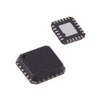
ADL5385ACPZ-R7 Analog Devices Inc, ADL5385ACPZ-R7 Datasheet

ADL5385ACPZ-R7
Specifications of ADL5385ACPZ-R7
Related parts for ADL5385ACPZ-R7
ADL5385ACPZ-R7 Summary of contents
Page 1
FEATURES Output frequency range: 50 MHz to 2200 MHz 1 dB output compression: 11 dBm @ 350 MHz Noise floor: –159 dBm/Hz @ 350 MHz Sideband suppression: −50 dBc @ 350 MHz Carrier feedthrough: −46 dBm @ 350 MHz Single ...
Page 2
ADL5385 TABLE OF CONTENTS Features .............................................................................................. 1 Applications....................................................................................... 1 Functional Block Diagram .............................................................. 1 Product Description......................................................................... 1 Specifications..................................................................................... 3 Absolute Maximum Ratings............................................................ 6 ESD Caution.................................................................................. 6 Pin Configuration and Functional Descriptions.......................... 7 Typical Performance Characteristics ............................................. 8 Circuit Description......................................................................... 12 ...
Page 3
SPECIFICATIONS Unless otherwise noted 25° −7 dBm; I/Q inputs = 1.4 V p-p differential sine waves in quadrature on a 500 bias; baseband frequency = 1 MHz; LO ...
Page 4
ADL5385 Parameter Conditions Second Baseband Harmonic (F − (2 × Third Baseband Harmonic ( × Output IP2 F1 = 3.5 MHz 4.5 MHz, P Output IP3 F1 = 3.5 MHz ...
Page 5
Parameter Conditions @ +85°C after optimization at +25°C @ −40°C after optimization at +25°C Second Baseband Harmonic (F − (2 × Third Baseband Harmonic ( × Output IP2 F1 = +3.5 MHz ...
Page 6
ADL5385 ABSOLUTE MAXIMUM RATINGS Table 2. Parameter Supply Voltage VPOS IBBP, IBBN, QBBP, QBBN Range LOIP and LOIN Internal Power Dissipation θ (Exposed Paddle Soldered Down) JA Maximum Junction Temperature Operating Temperature Range Storage Temperature Range ESD CAUTION Stresses above ...
Page 7
PIN CONFIGURATION AND FUNCTIONAL DESCRIPTIONS Table 3. Pin Function Descriptions Pin No. Mnemonic Description Connection. These pins can be left open or tied to ground 15, COM1, COM2, Power Supply Common Pins. ...
Page 8
ADL5385 TYPICAL PERFORMANCE CHARACTERISTICS Unless otherwise noted 25° −7 dBm; I/Q inputs = 1.4 V p-p differential sine waves in quadrature on a 500 mV dc bias baseband frequency = ...
Page 9
SSB OUTPUT POWER (dBm) CARRIER FEEDTHROUGH (dBm) SIDEBAND SUPPRESSION (dBc) SECOND-ORDER DISTORTION (dBc) –30 THIRD-ORDER DISTORTION (dBc) –40 –50 –60 –70 –80 0.2 0.6 1.0 1.4 1.8 2.2 BASEBAND AMPLITUDE (V p-p) Figure 9. SSB Output Power, Second- and ...
Page 10
ADL5385 –20 –30 –40 –50 –60 –70 –80 –90 –10 –8 –6 –4 – AMPLITUDE (dBm) Figure 15. Distribution of Sideband Suppression vs. LO Input Power at 50 MHz and 350 MHz –20 –30 –40 –50 –60 –70 ...
Page 11
AT 20MHz OFFSET FROM LO FREQUENCY Figure 21. 20 MHz Offset Noise Floor Distribution, Output Frequency = 350 MHz, ...
Page 12
ADL5385 CIRCUIT DESCRIPTION OVERVIEW The ADL5385 can be divided into five sections: the local oscillator (LO) interface, the baseband voltage-to-current (V-to-I) converter, the mixers, the differential-to-single-ended (D-to-S) amplifier, and the bias circuit. A detailed block diagram of the device is ...
Page 13
BASIC CONNECTIONS Figure 27 shows the basic connections for the ADL5385. QBBP QBBN IBBN RFPQ RFNQ RFNI CFPQ CFNQ CFNI 0Ω 0Ω 0Ω OPEN OPEN OPEN RTQ RTI OPEN OPEN 19 COM3 ENBL 12 VPS2 11 20 COM3 CLOP LO ...
Page 14
ADL5385 When an offset applied to the I-channel inputs, IOS V = 500 /2, while IOPP IOS V = 500 mV − V /2, such that IOPN IOS V − IOPP ...
Page 15
APPLICATIONS DAC MODULATOR INTERFACING The ADL5385 is designed to interface with minimal components to members of the Analog Devices family of digital-to-analog converters (DAC). These DACs feature an output current swing from mA, and the interface described ...
Page 16
ADL5385 Using AD9777 Auxiliary DAC for Carrier Feedthrough Nulling The AD9777 features an auxiliary DAC that can be used to inject small currents into the differential outputs for each channel. The auxiliary DAC can produce the small offset currents necessary ...
Page 17
ACPR2 (5.25MHz) –65 ACPR3 (6.00MHz) –70 ACPR1 (750kHz) –75 –80 MER –85 –90 –24 –22 –20 –18 –16 CARRIER POWER (dBm) Figure 38. ACP1, ACP2, ACP3, and Modulation Error Ratio (MER) vs. Output Power for 256 QAM ...
Page 18
ADL5385 LO GENERATION USING PLLs Analog Devices has a line of PLLs that can be used for generating the LO signal. Table 4 lists the PLLs together with their maximum frequency and phase noise performance. Table 4. PLL Selection Table ...
Page 19
EVALUATION BOARD A populated, RoHS-compliant ADL5385 evaluation board is available. The ADL5385 has an exposed paddle underneath the package, which is soldered to the board. The evaluation board is designed without any components on the underside so that heat can ...
Page 20
ADL5385 Yuping Toh Figure 42. Layout of Evaluation Board Rev Page ...
Page 21
CHARACTERIZATION SETUP SSB SETUP Figure diagram of the characterization test stand setup for the ADL5385, which is intended to test the product as a single-sideband modulator. The Aeroflex IFR3416 signal generator provides the I and Q inputs ...
Page 22
... INDICATOR 1.00 0.85 0.80 SEATING PLANE ORDERING GUIDE Model Temperature Range 1 ADL5385ACPZ-WP –40°C to +85°C ADL5385ACPZ-R2 1 –40°C to +85°C 1 ADL5385ACPZ-R7 –40°C to +85°C 1 ADL5385-EVALZ Pb-free part. 4.00 BSC SQ 0.60 MAX 0.50 BSC TOP 3.75 VIEW BSC SQ 0.50 0.40 ...
Page 23
NOTES Rev Page ADL5385 ...
Page 24
ADL5385 NOTES ©2006 Analog Devices, Inc. All rights reserved. Trademarks and registered trademarks are the property of their respective owners. D06118-0-10/06(0) Rev Page ...


