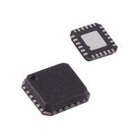
ADL5385ACPZ-R7 Analog Devices Inc, ADL5385ACPZ-R7 Datasheet - Page 14

ADL5385ACPZ-R7
Manufacturer Part Number
ADL5385ACPZ-R7
Description
IC, QUAD MODULATOR 50MHZ-2.2GHZ LFCSP-24
Manufacturer
Analog Devices Inc
Datasheet
1.ADL5385ACPZ-R7.pdf
(24 pages)
Specifications of ADL5385ACPZ-R7
Frequency Range
50MHz To 2.2GHz
Rf Type
Quadrature
Supply Voltage Range
4.75V To 5.5V
Rf Ic Case Style
LFCSP
No. Of Pins
24
Operating Temperature Range
-40°C To +85°C
Design Resources
Broadband Low EVM Direct Conversion Transmitter Using LO Divide-by-2 Modulator (CN0144)
Function
Modulator
Lo Frequency
50MHz ~ 2.2GHz
Rf Frequency
50MHz ~ 2.2GHz
P1db
8dBm
Noise Floor
-160dBm/Hz
Output Power
2.6dBm
Current - Supply
240mA
Voltage - Supply
4.75 V ~ 5.25 V
Test Frequency
2.15GHz
Package / Case
24-VFQFN, 24-CSP Exposed Pad
Rohs Compliant
Yes
Lead Free Status / RoHS Status
Lead free / RoHS Compliant
Other names
ADL5385ACPZ-R7TR
ADL5385
When an offset of +V
The same applies to the Q channel.
It is often desirable to perform a one-time carrier null
calibration. This is usually performed at a single frequency.
Figure 29 shows how carrier feedthrough varies with LO
frequency over a range of ±50 MHz on either side of a null at
350 MHz.
Figure 29. Carrier Feedthrough vs. Frequency After Nulling at 350 MHz
V
V
V
IOPP
IOPN
IOPP
–25
–30
–35
–40
–45
–50
–55
–60
–65
–70
–75
–80
–85
300
= 500 mV + V
− V
= 500 mV − V
IOPN
310
= V
320
IOS
IOS
330
OUTPUT FREQUENCY (MHz)
IOS
is applied to the I-channel inputs,
IOS
/2, while
/2, such that
340
350
360
370
380
390
400
Rev. 0 | Page 14 of 24
Sideband Suppression Optimization
Sideband suppression results from relative gain and relative
phase offsets between the I and Q channels and can be
suppressed through adjustments to those two parameters.
Figure 30 illustrates how sideband suppression is affected by the
gain and phase imbalances.
Figure 30 underscores the fact that adjusting one parameter
improves the sideband suppression only to a point; the other
parameter must also be adjusted. For example, if the amplitude
offset is 0.25 dB, improving the phase imbalance better than 1°
does not yield any improvement in the sideband suppression.
For optimum sideband suppression, an iterative adjustment
between phase and amplitude is required.
The sideband suppression nulling can be performed either through
adjusting the gain for each channel or through the modification
of the phase and gain of the digital data coming from the digital
signal processor.
Figure 30. Sideband Suppression vs. Quadrature Phase Error for Various
–10
–20
–30
–40
–50
–60
–70
–80
–90
0
0.01
2.5dB
1.25dB
0.5dB
0.25dB
0.125dB
0.05dB
0.025dB
0.0125dB
0dB
Quadrature Amplitude Offsets
0.1
PHASE ERROR (Degrees)
1
10
100


