PIC24FJ256GB106-I/MR Microchip Technology, PIC24FJ256GB106-I/MR Datasheet - Page 295
PIC24FJ256GB106-I/MR
Manufacturer Part Number
PIC24FJ256GB106-I/MR
Description
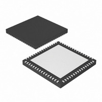
IC, 16BIT MCU, PIC24F, 32MHZ, QFN-64
Manufacturer
Microchip Technology
Series
PIC® 24Fr
Datasheets
1.PIC24FJ128GA106-IPT.pdf
(52 pages)
2.PIC24FJ64GB106-IPT.pdf
(16 pages)
3.PIC24FJ64GB106-IPT.pdf
(352 pages)
4.PIC24FJ192GB108-IPT.pdf
(328 pages)
Specifications of PIC24FJ256GB106-I/MR
Controller Family/series
PIC24
No. Of I/o's
51
Ram Memory Size
16KB
Cpu Speed
32MHz
No. Of Timers
5
Core Size
16 Bit
Program Memory Size
256KB
Peripherals
ADC, Comparator, PWM, RTC, Timer
Core Processor
PIC
Speed
32MHz
Connectivity
I²C, SPI, UART/USART, USB OTG
Number Of I /o
51
Program Memory Type
FLASH
Ram Size
16K x 8
Voltage - Supply (vcc/vdd)
2 V ~ 3.6 V
Data Converters
A/D 16x10b
Oscillator Type
Internal
Operating Temperature
-40°C ~ 85°C
Package / Case
64-VFQFN, Exposed Pad
Processor Series
PIC24FJ
Core
PIC
Data Bus Width
16 bit
Data Ram Size
16 KB
Interface Type
I2C, SPI, UART
Maximum Clock Frequency
32 MHz
Number Of Programmable I/os
52
Number Of Timers
5
Maximum Operating Temperature
+ 85 C
Mounting Style
SMD/SMT
3rd Party Development Tools
52713-733, 52714-737, 53276-922, EWDSPIC
Development Tools By Supplier
PG164130, DV164035, DV244005, DV164005, PG164120, DM240001, DM240011
Minimum Operating Temperature
- 40 C
On-chip Adc
10 bit, 16 Channel
Lead Free Status / RoHS Status
Lead free / RoHS Compliant
For Use With
876-1004 - PIC24 BREAKOUT BOARD
Eeprom Size
-
Lead Free Status / Rohs Status
Details
Available stocks
Company
Part Number
Manufacturer
Quantity
Price
Company:

Part Number:
PIC24FJ256GB106-I/MR
Manufacturer:
TI
Quantity:
1 292


26.3.1
The Watchdog Timer has an optional Fixed Window
mode of operation. In this Windowed mode, CLRWDT
instructions can only reset the WDT during the last 1/4
of the programmed WDT period. A CLRWDT instruction
executed before that window causes a WDT Reset,
similar to a WDT time-out.
Windowed WDT mode is enabled by programming the
WINDIS Configuration bit (CW1<6>) to ‘0’.
FIGURE 26-2:
26.4
PIC24FJ256GB110 family devices provide two compli-
mentary methods to protect application code from
overwrites and erasures. These also help to protect the
device from inadvertent configuration changes during
run time.
26.4.1
For all devices in the PIC24FJ256GB110 family, the
on-chip program memory space is treated as a single
block, known as the General Segment (GS). Code pro-
tection for this block is controlled by one Configuration
bit, GCP. This bit inhibits external reads and writes to
the program memory space. It has no direct effect in
normal execution mode.
Write protection is controlled by the GWRP bit in the
Configuration Word. When GWRP is programmed to
‘0’, internal write and erase operations to program
memory are blocked.
2009 Microchip Technology Inc.
Sleep or Idle Mode
New Clock Source
All Device Resets
CLRWDT Instr.
PWRSAV Instr.
Exit Sleep or
Transition to
LPRC Input
Program Verification and
Code Protection
Idle Mode
SWDTEN
FWDTEN
WINDOWED OPERATION
GENERAL SEGMENT PROTECTION
WDT BLOCK DIAGRAM
31 kHz
(5-bit/7-bit)
Prescaler
FWPSA
1 ms/4 ms
LPRC Control
PIC24FJ256GB110 FAMILY
Counter
WDT
26.3.2
The WDT is enabled or disabled by the FWDTEN
Configuration bit. When the FWDTEN Configuration bit
is set, the WDT is always enabled.
The WDT can be optionally controlled in software when
the FWDTEN Configuration bit has been programmed
to ‘0’. The WDT is enabled in software by setting the
SWDTEN control bit (RCON<5>). The SWDTEN
control bit is cleared on any device Reset. The software
WDT option allows the user to enable the WDT for
critical code segments and disable the WDT during
non-critical segments for maximum power savings.
26.4.2
In addition to global General Segment protection, a
separate subrange of the program memory space can
be individually protected against writes and erases.
This area can be used for many purposes where a sep-
arate block of write and erase protected code is
needed, such as bootloader applications. Unlike
common boot block implementations, the specially
protected segment in PIC24FJ256GB110 family
devices can be located by the user anywhere in the
program space, and configured in a wide range of
sizes.
Code segment protection provides an added level of
protection to a designated area of program memory, by
disabling the NVM safety interlock whenever a write or
erase address falls within a specified range. They do
not override General Segment protection controlled by
the GCP or GWRP bits. For example, if GCP and
GWRP are enabled, enabling segmented code protec-
tion for the bottom half of program memory does not
undo General Segment protection for the top half.
1:1 to 1:32.768
WDTPS<3:0>
Postscaler
CONTROL REGISTER
CODE SEGMENT PROTECTION
DS39897C-page 295
WDT Overflow
Wake from Sleep
Reset
Related parts for PIC24FJ256GB106-I/MR
Image
Part Number
Description
Manufacturer
Datasheet
Request
R

Part Number:
Description:
Manufacturer:
Microchip Technology Inc.
Datasheet:
Part Number:
Description:
Manufacturer:
Microchip Technology Inc.
Datasheet:
Part Number:
Description:
Manufacturer:
Microchip Technology Inc.
Datasheet:
Part Number:
Description:
Manufacturer:
Microchip Technology Inc.
Datasheet:
Part Number:
Description:
Manufacturer:
Microchip Technology Inc.
Datasheet:
Part Number:
Description:
Manufacturer:
Microchip Technology Inc.
Datasheet:
Part Number:
Description:
Manufacturer:
Microchip Technology Inc.
Datasheet:
Part Number:
Description:
Manufacturer:
Microchip Technology Inc.
Datasheet: