PIC24FJ256GB106-I/MR Microchip Technology, PIC24FJ256GB106-I/MR Datasheet - Page 179
PIC24FJ256GB106-I/MR
Manufacturer Part Number
PIC24FJ256GB106-I/MR
Description
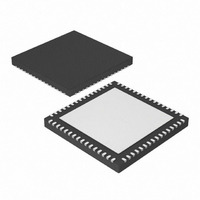
IC, 16BIT MCU, PIC24F, 32MHZ, QFN-64
Manufacturer
Microchip Technology
Series
PIC® 24Fr
Datasheets
1.PIC24FJ128GA106-IPT.pdf
(52 pages)
2.PIC24FJ64GB106-IPT.pdf
(16 pages)
3.PIC24FJ64GB106-IPT.pdf
(352 pages)
4.PIC24FJ192GB108-IPT.pdf
(328 pages)
Specifications of PIC24FJ256GB106-I/MR
Controller Family/series
PIC24
No. Of I/o's
51
Ram Memory Size
16KB
Cpu Speed
32MHz
No. Of Timers
5
Core Size
16 Bit
Program Memory Size
256KB
Peripherals
ADC, Comparator, PWM, RTC, Timer
Core Processor
PIC
Speed
32MHz
Connectivity
I²C, SPI, UART/USART, USB OTG
Number Of I /o
51
Program Memory Type
FLASH
Ram Size
16K x 8
Voltage - Supply (vcc/vdd)
2 V ~ 3.6 V
Data Converters
A/D 16x10b
Oscillator Type
Internal
Operating Temperature
-40°C ~ 85°C
Package / Case
64-VFQFN, Exposed Pad
Processor Series
PIC24FJ
Core
PIC
Data Bus Width
16 bit
Data Ram Size
16 KB
Interface Type
I2C, SPI, UART
Maximum Clock Frequency
32 MHz
Number Of Programmable I/os
52
Number Of Timers
5
Maximum Operating Temperature
+ 85 C
Mounting Style
SMD/SMT
3rd Party Development Tools
52713-733, 52714-737, 53276-922, EWDSPIC
Development Tools By Supplier
PG164130, DV164035, DV244005, DV164005, PG164120, DM240001, DM240011
Minimum Operating Temperature
- 40 C
On-chip Adc
10 bit, 16 Channel
Lead Free Status / RoHS Status
Lead free / RoHS Compliant
For Use With
876-1004 - PIC24 BREAKOUT BOARD
Eeprom Size
-
Lead Free Status / Rohs Status
Details
Available stocks
Company
Part Number
Manufacturer
Quantity
Price
Company:

Part Number:
PIC24FJ256GB106-I/MR
Manufacturer:
TI
Quantity:
1 292


REGISTER 14-2:
2009 Microchip Technology Inc.
bit 15
bit 7
Legend:
R = Readable bit
-n = Value at POR
bit 15
bit 14
bit 13
bit 12
bit 11-9
bit 8
bit 7
bit 6
bit 5
Note 1:
OCTRIG
FLTMD
R/W-0
R/W-0
2:
Never use an OC module as its own trigger source, either by selecting this mode or another equivalent
SYNCSEL setting.
Use these inputs as trigger sources only and never as sync sources.
FLTMD: Fault Mode Select bit
1 = Fault mode is maintained until the Fault source is removed and the corresponding OCFLT0 bit is
0 = Fault mode is maintained until the Fault source is removed and a new PWM period starts
FLTOUT: Fault Out bit
1 = PWM output is driven high on a Fault
0 = PWM output is driven low on a Fault
FLTTRIEN: Fault Output State Select bit
1 = Pin is forced to an output on a Fault condition
0 = Pin I/O condition is unaffected by a Fault
OCINV: OCMP Invert bit
1 = OCx output is inverted
0 = OCx output is not inverted
Unimplemented: Read as ‘0’
OC32: Cascade Two OC Modules Enable bit (32-bit operation)
1 = Cascade module operation enabled
0 = Cascade module operation disabled
OCTRIG: OCx Trigger/Sync Select bit
1 = Trigger OCx from source designated by the SYNCSELx bits
0 = Synchronize OCx with source designated by the SYNCSELx bits
TRIGSTAT: Timer Trigger Status bit
1 = Timer source has been triggered and is running
0 = Timer source has not been triggered and is being held clear
OCTRIS: OCx Output Pin Direction Select bit
1 = OCx pin is tristated
0 = Output compare peripheral x connected to OCx pin
TRIGSTAT
R/W-0 HS
FLTOUT
R/W-0
cleared in software
OCxCON2: OUTPUT COMPARE x CONTROL REGISTER 2
HS = Hardware Settable bit
W = Writable bit
‘1’ = Bit is set
FLTTRIEN
OCTRIS
R/W-0
R/W-0
SYNCSEL4
PIC24FJ256GB110 FAMILY
OCINV
R/W-0
R/W-0
U = Unimplemented bit, read as ‘0’
‘0’ = Bit is cleared
SYNCSEL3
R/W-1
U-0
—
SYNCSEL2
R/W-1
U-0
—
x = Bit is unknown
SYNCSEL1
R/W-0
U-0
—
DS39897C-page 179
SYNCSEL0
R/W-0
R/W-0
OC32
bit 8
bit 0
Related parts for PIC24FJ256GB106-I/MR
Image
Part Number
Description
Manufacturer
Datasheet
Request
R

Part Number:
Description:
Manufacturer:
Microchip Technology Inc.
Datasheet:
Part Number:
Description:
Manufacturer:
Microchip Technology Inc.
Datasheet:
Part Number:
Description:
Manufacturer:
Microchip Technology Inc.
Datasheet:
Part Number:
Description:
Manufacturer:
Microchip Technology Inc.
Datasheet:
Part Number:
Description:
Manufacturer:
Microchip Technology Inc.
Datasheet:
Part Number:
Description:
Manufacturer:
Microchip Technology Inc.
Datasheet:
Part Number:
Description:
Manufacturer:
Microchip Technology Inc.
Datasheet:
Part Number:
Description:
Manufacturer:
Microchip Technology Inc.
Datasheet: