PIC24FJ256GB106-I/MR Microchip Technology, PIC24FJ256GB106-I/MR Datasheet - Page 135
PIC24FJ256GB106-I/MR
Manufacturer Part Number
PIC24FJ256GB106-I/MR
Description
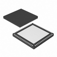
IC, 16BIT MCU, PIC24F, 32MHZ, QFN-64
Manufacturer
Microchip Technology
Series
PIC® 24Fr
Datasheets
1.PIC24FJ128GA106-IPT.pdf
(52 pages)
2.PIC24FJ64GB106-IPT.pdf
(16 pages)
3.PIC24FJ64GB106-IPT.pdf
(352 pages)
4.PIC24FJ192GB108-IPT.pdf
(328 pages)
Specifications of PIC24FJ256GB106-I/MR
Controller Family/series
PIC24
No. Of I/o's
51
Ram Memory Size
16KB
Cpu Speed
32MHz
No. Of Timers
5
Core Size
16 Bit
Program Memory Size
256KB
Peripherals
ADC, Comparator, PWM, RTC, Timer
Core Processor
PIC
Speed
32MHz
Connectivity
I²C, SPI, UART/USART, USB OTG
Number Of I /o
51
Program Memory Type
FLASH
Ram Size
16K x 8
Voltage - Supply (vcc/vdd)
2 V ~ 3.6 V
Data Converters
A/D 16x10b
Oscillator Type
Internal
Operating Temperature
-40°C ~ 85°C
Package / Case
64-VFQFN, Exposed Pad
Processor Series
PIC24FJ
Core
PIC
Data Bus Width
16 bit
Data Ram Size
16 KB
Interface Type
I2C, SPI, UART
Maximum Clock Frequency
32 MHz
Number Of Programmable I/os
52
Number Of Timers
5
Maximum Operating Temperature
+ 85 C
Mounting Style
SMD/SMT
3rd Party Development Tools
52713-733, 52714-737, 53276-922, EWDSPIC
Development Tools By Supplier
PG164130, DV164035, DV244005, DV164005, PG164120, DM240001, DM240011
Minimum Operating Temperature
- 40 C
On-chip Adc
10 bit, 16 Channel
Lead Free Status / RoHS Status
Lead free / RoHS Compliant
For Use With
876-1004 - PIC24 BREAKOUT BOARD
Eeprom Size
-
Lead Free Status / Rohs Status
Details
Available stocks
Company
Part Number
Manufacturer
Quantity
Price
Company:

Part Number:
PIC24FJ256GB106-I/MR
Manufacturer:
TI
Quantity:
1 292


10.3
The input change notification function of the I/O ports
allows the PIC24FJ256GB110 family of devices to
generate interrupt requests to the processor in
response to a Change-Of-State (COS) on selected
input pins. This feature is capable of detecting input
Change-Of-States even in Sleep mode, when the
clocks are disabled. Depending on the device pin
count, there are up to 81 external inputs that may be
selected (enabled) for generating an interrupt request
on a Change-Of-State.
Registers, CNEN1 through CNEN6, contain the inter-
rupt enable control bits for each of the CN input pins.
Setting any of these bits enables a CN interrupt for the
corresponding pins.
Each CN pin has a both a weak pull-up and a weak
pull-down connected to it. The pull-ups act as a current
source that is connected to the pin, while the
pull-downs act as a current sink that is connected to the
pin. These eliminate the need for external resistors
when push button or keypad devices are connected.
The pull-ups and pull-downs are separately enabled
using the CNPU1 through CNPU6 registers (for
pull-ups) and the CNPD1 through CNPD6 registers (for
pull-downs). Each CN pin has individual control bits for
its pull-up and pull-down. Setting a control bit enables
the weak pull-up or pull-down for the corresponding
pin.
When the internal pull-up is selected, the pin pulls up to
V
pull-up source when the internal pull-ups are enabled,
as the voltage difference can cause a current path.
2009 Microchip Technology Inc.
DD
Note:
– 0.7V (typical). Make sure that there is no external
Input Change Notification
Pull-ups on change notification pins
should always be disabled whenever the
port pin is configured as a digital output.
PIC24FJ256GB110 FAMILY
10.4
A major challenge in general purpose devices is provid-
ing the largest possible set of peripheral features while
minimizing the conflict of features on I/O pins. In an
application that needs to use more than one peripheral
multiplexed on a single pin, inconvenient workarounds
in application code or a complete redesign may be the
only option.
The Peripheral Pin Select (PPS) feature provides an
alternative to these choices by enabling the user’s
peripheral set selection and their placement on a wide
range of I/O pins. By increasing the pinout options
available on a particular device, users can better tailor
the microcontroller to their entire application, rather
than trimming the application to fit the device.
The Peripheral Pin Select feature operates over a fixed
subset of digital I/O pins. Users may independently
map the input and/or output of any one of many digital
peripherals to any one of these I/O pins. Peripheral Pin
Select is performed in software and generally does not
require the device to be reprogrammed. Hardware
safeguards are included that prevent accidental or
spurious changes to the peripheral mapping once it has
been established.
10.4.1
The Peripheral Pin Select feature is used with a range
of up to 44 pins, depending on the particular device and
its pin count. Pins that support the Peripheral Pin
Select feature include the designation, “RPn” or “RPIn”,
in their full pin designation, where “n” is the remappable
pin number. “RP” is used to designate pins that support
both remappable input and output functions, while
“RPI” indicates pins that support remappable input
functions only.
PIC24FJ256GB110 family devices support a larger
number of remappable input only pins than remappable
input/output pins. In this device family, there are up to
32 remappable input/output pins, depending on the pin
count of the particular device selected; these are num-
bered, RP0 through RP31. Remappable input only pins
are numbered above this range, from RPI32 to RPI43
(or the upper limit for that particular device).
See Table 1-4 for a summary of pinout options in each
package offering.
Peripheral Pin Select
AVAILABLE PINS
DS39897C-page 135
Related parts for PIC24FJ256GB106-I/MR
Image
Part Number
Description
Manufacturer
Datasheet
Request
R

Part Number:
Description:
Manufacturer:
Microchip Technology Inc.
Datasheet:
Part Number:
Description:
Manufacturer:
Microchip Technology Inc.
Datasheet:
Part Number:
Description:
Manufacturer:
Microchip Technology Inc.
Datasheet:
Part Number:
Description:
Manufacturer:
Microchip Technology Inc.
Datasheet:
Part Number:
Description:
Manufacturer:
Microchip Technology Inc.
Datasheet:
Part Number:
Description:
Manufacturer:
Microchip Technology Inc.
Datasheet:
Part Number:
Description:
Manufacturer:
Microchip Technology Inc.
Datasheet:
Part Number:
Description:
Manufacturer:
Microchip Technology Inc.
Datasheet: