PIC24FJ256GB106-I/MR Microchip Technology, PIC24FJ256GB106-I/MR Datasheet - Page 291
PIC24FJ256GB106-I/MR
Manufacturer Part Number
PIC24FJ256GB106-I/MR
Description
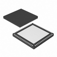
IC, 16BIT MCU, PIC24F, 32MHZ, QFN-64
Manufacturer
Microchip Technology
Series
PIC® 24Fr
Datasheets
1.PIC24FJ128GA106-IPT.pdf
(52 pages)
2.PIC24FJ64GB106-IPT.pdf
(16 pages)
3.PIC24FJ64GB106-IPT.pdf
(352 pages)
4.PIC24FJ192GB108-IPT.pdf
(328 pages)
Specifications of PIC24FJ256GB106-I/MR
Controller Family/series
PIC24
No. Of I/o's
51
Ram Memory Size
16KB
Cpu Speed
32MHz
No. Of Timers
5
Core Size
16 Bit
Program Memory Size
256KB
Peripherals
ADC, Comparator, PWM, RTC, Timer
Core Processor
PIC
Speed
32MHz
Connectivity
I²C, SPI, UART/USART, USB OTG
Number Of I /o
51
Program Memory Type
FLASH
Ram Size
16K x 8
Voltage - Supply (vcc/vdd)
2 V ~ 3.6 V
Data Converters
A/D 16x10b
Oscillator Type
Internal
Operating Temperature
-40°C ~ 85°C
Package / Case
64-VFQFN, Exposed Pad
Processor Series
PIC24FJ
Core
PIC
Data Bus Width
16 bit
Data Ram Size
16 KB
Interface Type
I2C, SPI, UART
Maximum Clock Frequency
32 MHz
Number Of Programmable I/os
52
Number Of Timers
5
Maximum Operating Temperature
+ 85 C
Mounting Style
SMD/SMT
3rd Party Development Tools
52713-733, 52714-737, 53276-922, EWDSPIC
Development Tools By Supplier
PG164130, DV164035, DV244005, DV164005, PG164120, DM240001, DM240011
Minimum Operating Temperature
- 40 C
On-chip Adc
10 bit, 16 Channel
Lead Free Status / RoHS Status
Lead free / RoHS Compliant
For Use With
876-1004 - PIC24 BREAKOUT BOARD
Eeprom Size
-
Lead Free Status / Rohs Status
Details
Available stocks
Company
Part Number
Manufacturer
Quantity
Price
Company:

Part Number:
PIC24FJ256GB106-I/MR
Manufacturer:
TI
Quantity:
1 292


REGISTER 26-2:
REGISTER 26-3:
2009 Microchip Technology Inc.
bit 4
bit 3
bit 2
bit 1-0
bit 23
bit 15
bit 7
Legend:
R = Readable bit
-n = Value when device is unprogrammed
bit 23-16
bit 15
bit 14
bit 13
bit 12-8
bit 7-0
WPEND
WPFP7
R/PO-1
R/PO-1
U-1
—
IOL1WAY: IOLOCK One-Way Set Enable bit
1 = The IOLOCK bit (OSCCON<6>)can be set once, provided the unlock sequence has been
0 = The IOLOCK bit can be set and cleared as needed, provided the unlock sequence has been
DISUVREG: Internal USB 3.3V Regulator Disable bit
1 = Regulator is disabled
0 = Regulator is enabled
Reserved: Always maintain as ‘1’
POSCMD<1:0>: Primary Oscillator Configuration bits
11 = Primary Oscillator disabled
10 = HS Oscillator mode selected
01 = XT Oscillator mode selected
00 = EC Oscillator mode selected
Unimplemented: Read as ‘1’
WPEND: Segment Write Protection End Page Select bit
1 = Protected code segment lower boundary is at the bottom of program memory (000000h); upper
0 = Protected code segment upper boundary is at the last page of program memory; lower boundary
WPCFG: Configuration Word Code Page Protection Select bit
1 = Last page (at the top of program memory) and Flash Configuration Words are not protected
0 = Last page and Flash Configuration Words are code protected
WPDIS: Segment Write Protection Disable bit
1 = Segmented code protection disabled
0 = Segmented code protection enabled; protected segment defined by WPEND, WPCFG and
Unimplemented: Read as ‘1’
WPFP<7:0>: Protected Code Segment Boundary Page bits
Designates the 512-word program code page that is the boundary of the protected code segment,
starting with Page 0 at the bottom of program memory.
If WPEND = 1:
Last address of designated code page is the upper boundary of the segment.
If WPEND = ‘0’:
First address of designated code page is the lower boundary of the segment.
WPCFG
WPFP6
R/PO-1
R/PO-1
completed. Once set, the Peripheral Pin Select registers cannot be written to a second time.
completed
boundary is the code page specified by WPFP<7:0>
is the code page specified by WPFP<7:0>
WPFPx Configuration bits
U-1
—
CW2: FLASH CONFIGURATION WORD 2 (CONTINUED)
CW3: FLASH CONFIGURATION WORD 3
PO = Program-once bit
WPFP5
R/PO-1
R/PO-1
WPDIS
U-1
—
PIC24FJ256GB110 FAMILY
WPFP4
R/PO-1
U-1
U-1
—
—
U = Unimplemented bit, read as ‘0’
‘1’ = Bit is set
R/PO-1
WPFP3
U-1
U-1
—
—
WPFP2
R/PO-1
U-1
U-1
—
—
‘0’ = Bit is cleared
WPFP1
R/PO-1
U-1
U-1
—
—
DS39897C-page 291
WPFP0
R/PO-1
U-1
U-1
—
—
bit 16
bit 8
bit 0
Related parts for PIC24FJ256GB106-I/MR
Image
Part Number
Description
Manufacturer
Datasheet
Request
R

Part Number:
Description:
Manufacturer:
Microchip Technology Inc.
Datasheet:
Part Number:
Description:
Manufacturer:
Microchip Technology Inc.
Datasheet:
Part Number:
Description:
Manufacturer:
Microchip Technology Inc.
Datasheet:
Part Number:
Description:
Manufacturer:
Microchip Technology Inc.
Datasheet:
Part Number:
Description:
Manufacturer:
Microchip Technology Inc.
Datasheet:
Part Number:
Description:
Manufacturer:
Microchip Technology Inc.
Datasheet:
Part Number:
Description:
Manufacturer:
Microchip Technology Inc.
Datasheet:
Part Number:
Description:
Manufacturer:
Microchip Technology Inc.
Datasheet: