PIC24FJ256GB106-I/MR Microchip Technology, PIC24FJ256GB106-I/MR Datasheet - Page 122
PIC24FJ256GB106-I/MR
Manufacturer Part Number
PIC24FJ256GB106-I/MR
Description
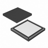
IC, 16BIT MCU, PIC24F, 32MHZ, QFN-64
Manufacturer
Microchip Technology
Series
PIC® 24Fr
Datasheets
1.PIC24FJ128GA106-IPT.pdf
(52 pages)
2.PIC24FJ64GB106-IPT.pdf
(16 pages)
3.PIC24FJ64GB106-IPT.pdf
(352 pages)
4.PIC24FJ192GB108-IPT.pdf
(328 pages)
Specifications of PIC24FJ256GB106-I/MR
Controller Family/series
PIC24
No. Of I/o's
51
Ram Memory Size
16KB
Cpu Speed
32MHz
No. Of Timers
5
Core Size
16 Bit
Program Memory Size
256KB
Peripherals
ADC, Comparator, PWM, RTC, Timer
Core Processor
PIC
Speed
32MHz
Connectivity
I²C, SPI, UART/USART, USB OTG
Number Of I /o
51
Program Memory Type
FLASH
Ram Size
16K x 8
Voltage - Supply (vcc/vdd)
2 V ~ 3.6 V
Data Converters
A/D 16x10b
Oscillator Type
Internal
Operating Temperature
-40°C ~ 85°C
Package / Case
64-VFQFN, Exposed Pad
Processor Series
PIC24FJ
Core
PIC
Data Bus Width
16 bit
Data Ram Size
16 KB
Interface Type
I2C, SPI, UART
Maximum Clock Frequency
32 MHz
Number Of Programmable I/os
52
Number Of Timers
5
Maximum Operating Temperature
+ 85 C
Mounting Style
SMD/SMT
3rd Party Development Tools
52713-733, 52714-737, 53276-922, EWDSPIC
Development Tools By Supplier
PG164130, DV164035, DV244005, DV164005, PG164120, DM240001, DM240011
Minimum Operating Temperature
- 40 C
On-chip Adc
10 bit, 16 Channel
Lead Free Status / RoHS Status
Lead free / RoHS Compliant
For Use With
876-1004 - PIC24 BREAKOUT BOARD
Eeprom Size
-
Lead Free Status / Rohs Status
Details
Available stocks
Company
Part Number
Manufacturer
Quantity
Price
Company:

Part Number:
PIC24FJ256GB106-I/MR
Manufacturer:
TI
Quantity:
1 292


PIC24FJ256GB110 FAMILY
8.1
The system clock source can be provided by one of
four sources:
• Primary Oscillator (POSC) on the OSCI and
• Secondary Oscillator (SOSC) on the SOSCI and
• Fast Internal RC (FRC) Oscillator
• Low-Power Internal RC (LPRC) Oscillator
The Primary Oscillator and FRC sources have the
option of using the internal USB PLL block, which
generates both the USB module clock and a separate
system clock from the 96 MHZ PLL. Refer to
Section 8.5 “Oscillator Modes and USB Operation”
for additional information.
The Fast Internal FRC provides an 8 MHz clock
source. It can optionally be reduced by the programma-
ble clock divider to provide a range of system clock
frequencies.
The selected clock source generates the processor and
peripheral clock sources. The processor clock source is
divided by two to produce the internal instruction cycle
clock, F
is also denoted by F
clock, F
some operating modes of the Primary Oscillator.
TABLE 8-1:
DS39897C-page 122
Fast RC Oscillator with Postscaler
(FRCDIV)
(Reserved)
Low-Power RC Oscillator (LPRC)
Secondary (Timer1) Oscillator
(SOSC)
Primary Oscillator (XT) with PLL
Module (XTPLL)
Primary Oscillator (EC) with PLL
Module (ECPLL)
Primary Oscillator (HS)
Primary Oscillator (XT)
Primary Oscillator (EC)
Fast RC Oscillator with PLL Module
(FRCPLL)
Fast RC Oscillator (FRC)
Note 1:
OSCO pins
SOSCO pins
2:
OSC
CY
CPU Clocking Scheme
. In this document, the instruction cycle clock
Oscillator Mode
/2, can be provided on the OSCO I/O pin for
OSCO pin function is determined by the OSCIOFCN Configuration bit.
This is the default oscillator mode for an unprogrammed (erased) device.
CONFIGURATION BIT VALUES FOR CLOCK SELECTION
OSC
/2. The internal instruction cycle
Oscillator Source
Secondary
Primary
Primary
Primary
Primary
Primary
Internal
Internal
Internal
Internal
Internal
Configuration bit settings. The oscillator Configuration
8.2
The oscillator source (and operating mode) that is used
at a device Power-on Reset event is selected using
bit settings are located in the Configuration registers in
the program memory (refer to Section 26.1 “Configu-
ration Bits” for further details). The Primary Oscillator
Configuration
Word 2<1:0>), and the Initial Oscillator Select Configu-
ration bits, FNOSC<2:0> (Configuration Word 2<10:8>),
select the oscillator source that is used at a Power-on
Reset. The FRC Primary Oscillator with Postscaler
(FRCDIV) is the default (unprogrammed) selection. The
Secondary Oscillator, or one of the internal oscillators,
may be chosen by programming these bit locations.
The Configuration bits allow users to choose between
the various clock modes, shown in Table 8-1.
8.2.1
The
Word 2<7:6>) are used to jointly configure device clock
switching and the Fail-Safe Clock Monitor (FSCM).
Clock switching is enabled only when FCKSM1 is
programmed (‘0’). The FSCM is enabled only when
FCKSM<1:0> are both programmed (‘00’).
POSCMD<1:0>
FCKSM
11
xx
11
11
01
00
10
01
00
11
11
Initial Configuration on POR
CLOCK SWITCHING MODE
CONFIGURATION BITS
bits,
Configuration
POSCMD<1:0>
2009 Microchip Technology Inc.
FNOSC<2:0>
111
110
101
100
011
011
010
010
010
001
000
bits
(Configuration
(Configuration
Note
1, 2
1
1
1
1
1
Related parts for PIC24FJ256GB106-I/MR
Image
Part Number
Description
Manufacturer
Datasheet
Request
R

Part Number:
Description:
Manufacturer:
Microchip Technology Inc.
Datasheet:
Part Number:
Description:
Manufacturer:
Microchip Technology Inc.
Datasheet:
Part Number:
Description:
Manufacturer:
Microchip Technology Inc.
Datasheet:
Part Number:
Description:
Manufacturer:
Microchip Technology Inc.
Datasheet:
Part Number:
Description:
Manufacturer:
Microchip Technology Inc.
Datasheet:
Part Number:
Description:
Manufacturer:
Microchip Technology Inc.
Datasheet:
Part Number:
Description:
Manufacturer:
Microchip Technology Inc.
Datasheet:
Part Number:
Description:
Manufacturer:
Microchip Technology Inc.
Datasheet: