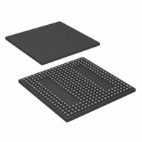
ADSP-BF538BBCZ-5F4 Analog Devices Inc, ADSP-BF538BBCZ-5F4 Datasheet - Page 16

ADSP-BF538BBCZ-5F4
Manufacturer Part Number
ADSP-BF538BBCZ-5F4
Description
IC, FLOAT-PT DSP, 16BIT, 533MHZ, BGA-316
Manufacturer
Analog Devices Inc
Series
Blackfinr
Type
Fixed Pointr
Specifications of ADSP-BF538BBCZ-5F4
No. Of Bits
16 Bit
Frequency
533MHz
Supply Voltage
1.25V
Embedded Interface Type
CAN, I2C, PPI, SPI, TWI, UART
No. Of I/o's
54
Flash Memory Size
512KB
Interface
CAN, SPI, SSP, TWI, UART
Clock Rate
533MHz
Non-volatile Memory
FLASH (512 kB)
On-chip Ram
148kB
Voltage - I/o
3.00V, 3.30V
Voltage - Core
1.25V
Operating Temperature
-40°C ~ 85°C
Mounting Type
Surface Mount
Package / Case
316-CSPBGA
Lead Free Status / RoHS Status
Lead free / RoHS Compliant
For Use With
ADZS-BFAUDIO-EZEXT - BOARD EVAL AUDIO BLACKFIN
Lead Free Status / RoHS Status
Lead free / RoHS Compliant, Lead free / RoHS Compliant
ADSP-BF538/ADSP-BF538F
Table 7
Table 7. Example System Clock Ratios
The maximum frequency of the system clock is f
the divisor ratio must be chosen to limit the system clock fre-
quency to its maximum of f
dynamically without any PLL lock latencies by writing the
appropriate values to the PLL divisor register (PLL_DIV).
Note that when the SSEL value is changed, it will affect all the
peripherals that derive their clock signals from the SCLK signal.
The core clock (CCLK) frequency can also be dynamically
changed by means of the CSEL1–0 bits of the PLL_DIV register.
Supported CCLK divider ratios are 1, 2, 4, and 8, as shown in
Table
fast core frequency modifications.
Table 8. Core Clock Ratios
BOOTING MODES
The ADSP-BF538/ADSP-BF538F processors have three mecha-
nisms (listed in
instruction memory after a reset. A fourth mode is provided to
execute from external memory, bypassing the boot sequence.
Table 9. Booting Modes
Signal Name
SSEL3–0
0001
0110
1010
Signal Name
CSEL1–0
00
01
10
11
BMODE1–0 Description
00
01
10
11
8. This programmable core clock capability is useful for
illustrates typical system clock ratios:
Execute from 16-Bit External Memory
(Bypass Boot ROM)
Boot from 8-Bit or 16-Bit Flash, or
Boot from On-Chip Flash (ADSP-BF538F Only)
Boot from SPI Serial Master Connected to SPI0
Boot from SPI Serial Slave EEPROM /Flash
(8-,16-, or 24-Bit Address Range, or Atmel
AT45DB041, AT45DB081, or AT45DB161 Serial Flash)
Connected to SPI0
Divider Ratio
VCO/SCLK
1:1
6:1
10:1
Table
Divider Ratio
VCO/CCLK
1:1
2:1
4:1
8:1
9) for automatically loading internal L1
SCLK
. The SSEL value can be changed
Example Frequency Ratios (MHz)
VCO
100
300
500
Example Frequency Ratios
VCO
300
300
500
200
SCLK
100
50
50
CCLK
300
150
125
25
SCLK
Rev. A | Page 16 of 56 | January 2008
. Note that
The BMODE pins of the reset configuration register, sampled
during power-on resets and software initiated resets, implement
the following modes:
For each of the boot modes, a 10-byte header is first read from
an external memory device. The header specifies the number of
bytes to be transferred and the memory destination address.
Multiple memory blocks may be loaded by any boot sequence.
Once all blocks are loaded, program execution commences from
the start of L1 instruction SRAM.
In addition, Bit 4 of the reset configuration register can be set by
application code to bypass the normal boot sequence during a
software reset. For this case, the processor jumps directly to the
beginning of L1 instruction memory.
To augment the boot modes, a secondary software loader is pro-
vided that adds additional booting mechanisms. This secondary
loader provides the capability to boot from 16-bit flash memory,
fast flash, variable baud rate, and other sources. In all boot
modes except bypass, program execution starts from on-chip L1
memory address 0xFFA0 0000.
INSTRUCTION SET DESCRIPTION
The Blackfin processor family assembly language instruction set
employs an algebraic syntax designed for ease of coding and
readability. The instructions have been specifically tuned to pro-
vide a flexible, densely encoded instruction set that compiles to
a very small final memory size. The instruction set also provides
• Execute from 16-bit external memory – Execution starts
• Boot from 8-bit or 16-bit external flash memory – The 8-bit
• Boot from SPI serial EEPROM/flash (8-, 16-, or 24-bit
• Boot from SPI host device connected to SPI0 – The Black-
from address 0x2000 0000 with 16-bit packing. The boot
ROM is bypassed in this mode. All configuration settings
are set for the slowest device possible (3-cycle hold time;
15-cycle R/W access times; 4-cycle setup).
flash boot routine located in boot ROM memory space is
set up using asynchronous memory bank 0. For
ADSP-BF538F processors, the on-chip flash is booted if
FCE is connected to AMS0. All configuration settings are
set for the slowest device possible (3-cycle hold time;
15-cycle R/W access times; 4-cycle setup).
addressable, or Atmel AT45DB041, AT45DB081, or
AT45DB161) connected to SPI0– SPI0 uses the PF2 output
pin to select a single SPI EEPROM/flash device, submits a
read command and successive address bytes (0x00) until a
valid 8-, 16-, or 24-bit, or Atmel addressable device is
detected, and begins clocking data into the processor at the
beginning of L1 instruction memory.
fin processor operates in SPI slave mode and is configured
to receive the bytes of the LDR file from an SPI host (mas-
ter) agent. To hold off the host device from transmitting
while the boot ROM is busy, the Blackfin processor asserts
a GPIO pin, called host wait (HWAIT), to signal the host
device not to send any more bytes until the flag is deas-
serted. The flag is chosen by the user and this information
is transferred to the Blackfin processor via bits 10:5 of the
FLAG header in the LDR image.


