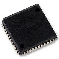
SC16C2552BIA44 NXP Semiconductors, SC16C2552BIA44 Datasheet - Page 8

SC16C2552BIA44
Manufacturer Part Number
SC16C2552BIA44
Description
UART, 2 CH, 16BYTE FIFO, 16C2552
Manufacturer
NXP Semiconductors
Datasheet
1.SC16C2552BIA44.pdf
(38 pages)
Specifications of SC16C2552BIA44
No. Of Channels
2
Data Rate
5Mbps
Supply Voltage Range
2.25V To 5.5V
Operating Temperature Range
-40°C To +85°C
Digital Ic Case Style
PLCC
No. Of Pins
44
Svhc
No SVHC (18-Jun-2010)
Operating
RoHS Compliant
Uart Features
Independent Transmit & Receive UART Control, Multi-Function Output, Modem Control Functions
Rohs Compliant
Yes
Available stocks
Company
Part Number
Manufacturer
Quantity
Price
Part Number:
SC16C2552BIA44
Manufacturer:
NXP/恩智浦
Quantity:
20 000
Company:
Part Number:
SC16C2552BIA44,529
Manufacturer:
NXP Semiconductors
Quantity:
10 000
NXP Semiconductors
SC16C2552B_3
Product data sheet
6.5 Programmable baud rate generator
When two interrupt conditions have the same priority, it is important to service these
interrupts correctly. Receive Data Ready and Receive Time-Out have the same interrupt
priority (when enabled by IER[0]). The receiver issues an interrupt after the number of
characters have reached the programmed trigger level. In this case, the SC16C2552B
FIFO may hold more characters than the programmed trigger level. Following the removal
of a data byte, the user should re-check LSR[0] for additional characters. A Receive
Time-Out will not occur if the receive FIFO is empty. The time-out counter is reset at the
center of each stop bit received or each time the receive holding register (RHR) is read.
The actual time-out value is 4 character time.
The SC16C2552B supports high speed modem technologies that have increased input
data rates by employing data compression schemes. For example, a 33.6 kbit/s modem
that employs data compression may require a 115.2 kbit/s input data rate. A 128.0 kbit/s
ISDN modem that supports data compression may need an input data rate of 460.8 kbit/s.
A baud rate generator is provided for each UART channel, allowing independent TX/RX
channel control. The programmable Baud Rate Generator (BRG) is capable of accepting
an input clock up to 80 MHz, as required for supporting a 5 Mbit/s data rate. The
SC16C2552B can be configured for internal or external clock operation. For internal clock
oscillator operation, an industry standard microprocessor crystal is connected externally
between the XTAL1 and XTAL2 pins. Alternatively, an external clock can be connected to
the XTAL1 pin to clock the internal baud rate generator for standard or custom rates (see
Table
The generator divides the input 16 clock by any divisor from 1 to (2
SC16C2552B divides the basic external clock by 16. The basic 16 clock provides table
rates to support standard and custom applications using the same system design. The
rate table is configured via the DLL and DLM internal register functions. Customized baud
rates can be achieved by selecting the proper divisor values for the MSB and LSB
sections of baud rate generator.
Programming the baud rate generator registers DLM (MSB) and DLL (LSB) provides a
user capability for selecting the desired final baud rate. The example in
selectable baud rate table available when using a 1.8432 MHz external clock input.
Fig 3.
5).
Crystal oscillator connection
5 V, 3.3 V and 2.5 V dual UART, 5 Mbit/s (max.), with 16-byte FIFOs
Rev. 03 — 12 February 2009
XTAL1
1.8432 MHz
C1
22 pF
X1
XTAL2
002aab325
C2
33 pF
SC16C2552B
16
Table 5
© NXP B.V. 2009. All rights reserved.
1). The
shows the
8 of 38


