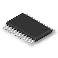
PCA9555PW NXP Semiconductors, PCA9555PW Datasheet - Page 15

PCA9555PW
Manufacturer Part Number
PCA9555PW
Description
IC, I2C-BUS AND SMBUS I/O PORT, TSSOP24
Manufacturer
NXP Semiconductors
Datasheet
1.PCA9555BS118.pdf
(34 pages)
Specifications of PCA9555PW
Chip Configuration
16 Bit
Bus Frequency
400kHz
Ic Interface Type
I2C
No. Of I/o's
16
Supply Voltage Range
2.3V To 5.5V
Digital Ic Case Style
TSSOP
No. Of Pins
24
Termination Type
SMD
Filter Terminals
SMD
Rohs Compliant
Yes
Lead Free Status / RoHS Status
Lead free / RoHS Compliant
Available stocks
Company
Part Number
Manufacturer
Quantity
Price
Company:
Part Number:
PCA9555PW
Manufacturer:
NXP
Quantity:
3 125
Company:
Part Number:
PCA9555PW
Manufacturer:
NXP Semiconductors
Quantity:
36 610
Part Number:
PCA9555PW
Manufacturer:
PHILIPS
Quantity:
20 000
Company:
Part Number:
PCA9555PW/G
Manufacturer:
MPS
Quantity:
23 062
Part Number:
PCA9555PW/G118
Manufacturer:
PHILIPS/飞利浦
Quantity:
20 000
Part Number:
PCA9555PWR
Manufacturer:
TI/德州仪器
Quantity:
20 000
Part Number:
PCA9555PWRG4
Manufacturer:
TI/德州仪器
Quantity:
20 000
NXP Semiconductors
PCA9555_8
Product data sheet
Fig 17. System configuration
SDA
SCL
TRANSMITTER/
RECEIVER
MASTER
7.2 System configuration
7.3 Acknowledge
A device generating a message is a ‘transmitter’; a device receiving is the ‘receiver’. The
device that controls the message is the ‘master’ and the devices which are controlled by
the master are the ‘slaves’ (see
The number of data bytes transferred between the START and the STOP conditions from
transmitter to receiver is not limited. Each byte of eight bits is followed by one
acknowledge bit. The acknowledge bit is a HIGH level put on the bus by the transmitter,
whereas the master generates an extra acknowledge related clock pulse.
A slave receiver which is addressed must generate an acknowledge after the reception of
each byte. Also a master must generate an acknowledge after the reception of each byte
that has been clocked out of the slave transmitter. The device that acknowledges has to
pull down the SDA line during the acknowledge clock pulse, so that the SDA line is stable
LOW during the HIGH period of the acknowledge related clock pulse; set-up time and hold
time must be taken into account.
A master receiver must signal an end of data to the transmitter by not generating an
acknowledge on the last byte that has been clocked out of the slave. In this event, the
transmitter must leave the data line HIGH to enable the master to generate a STOP
condition.
Fig 18. Acknowledgement on the I
RECEIVER
SLAVE
SCL from master
by transmitter
data output
by receiver
data output
Rev. 08 — 22 October 2009
TRANSMITTER/
RECEIVER
condition
START
SLAVE
S
Figure
2
C-bus
TRANSMITTER
1
16-bit I
17).
MASTER
2
C-bus and SMBus I/O port with interrupt
2
TRANSMITTER/
RECEIVER
MASTER
acknowledgement
not acknowledge
SLAVE
clock pulse for
acknowledge
8
MULTIPLEXER
PCA9555
© NXP B.V. 2009. All rights reserved.
002aaa987
I
2
9
C-BUS
002aaa966
15 of 34


