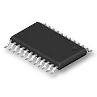
PCA9555PW NXP Semiconductors, PCA9555PW Datasheet - Page 11

PCA9555PW
Manufacturer Part Number
PCA9555PW
Description
IC, I2C-BUS AND SMBUS I/O PORT, TSSOP24
Manufacturer
NXP Semiconductors
Datasheet
1.PCA9555BS118.pdf
(34 pages)
Specifications of PCA9555PW
Chip Configuration
16 Bit
Bus Frequency
400kHz
Ic Interface Type
I2C
No. Of I/o's
16
Supply Voltage Range
2.3V To 5.5V
Digital Ic Case Style
TSSOP
No. Of Pins
24
Termination Type
SMD
Filter Terminals
SMD
Rohs Compliant
Yes
Lead Free Status / RoHS Status
Lead free / RoHS Compliant
Available stocks
Company
Part Number
Manufacturer
Quantity
Price
Company:
Part Number:
PCA9555PW
Manufacturer:
NXP
Quantity:
3 125
Company:
Part Number:
PCA9555PW
Manufacturer:
NXP Semiconductors
Quantity:
36 610
Part Number:
PCA9555PW
Manufacturer:
PHILIPS
Quantity:
20 000
Company:
Part Number:
PCA9555PW/G
Manufacturer:
MPS
Quantity:
23 062
Part Number:
PCA9555PW/G118
Manufacturer:
PHILIPS/飞利浦
Quantity:
20 000
Part Number:
PCA9555PWR
Manufacturer:
TI/德州仪器
Quantity:
20 000
Part Number:
PCA9555PWRG4
Manufacturer:
TI/德州仪器
Quantity:
20 000
NXP Semiconductors
PCA9555_8
Product data sheet
Fig 12. Read from register
SDA
(cont.)
Remark: Transfer can be stopped at any time by a STOP condition.
S
START condition
S
(repeated)
START condition
6.5.2 Reading the port registers
0
0
1
slave address
1
0
slave address
0
In order to read data from the PCA9555, the bus master must first send the PCA9555
address with the least significant bit set to a logic 0 (see
address”). The command byte is sent after the address and determines which register will
be accessed. After a restart, the device address is sent again, but this time the least
significant bit is set to a logic 1. Data from the register defined by the command byte will
then be sent by the PCA9555 (see
into the register on the falling edge of the acknowledge clock pulse. After the first byte is
read, additional bytes may be read but the data will now reflect the information in the other
register in the pair. For example, if you read Input Port 1, then the next byte read would be
Input Port 0. There is no limitation on the number of data bytes received in one read
transmission but the final byte received, the bus master must not acknowledge the data.
0 A2 A1 A0
0 A2 A1 A0 1
acknowledge
from slave
acknowledge
R/W
from slave
0
R/W
A
A
MSB
Rev. 08 — 22 October 2009
COMMAND BYTE
at this moment master-transmitter becomes master-receiver
and slave-receiver becomes slave-transmitter
upper byte of register
data from lower or
DATA (first byte)
acknowledge
from slave
Figure
16-bit I
LSB
A
12,
A
acknowledge
from master
(cont.)
2
Figure 13
C-bus and SMBus I/O port with interrupt
MSB
lower byte of register
data from upper or
DATA (last byte)
and
Figure 8 “PCA9555 device
Figure
no acknowledge
from master
14). Data is clocked
LSB
PCA9555
© NXP B.V. 2009. All rights reserved.
NA
002aac222
P
STOP
condition
11 of 34


