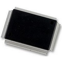
LM97593VH National Semiconductor, LM97593VH Datasheet - Page 47

LM97593VH
Manufacturer Part Number
LM97593VH
Description
12BIT ADC, 2CH, DDC/AGC, 128PQFP
Manufacturer
National Semiconductor
Datasheet
1.LM97593VH.pdf
(50 pages)
Specifications of LM97593VH
Resolution (bits)
12bit
Input Channel Type
Differential
Data Interface
Serial
Supply Voltage Range - Analogue
3V To 3.6V
Supply Voltage Range - Digital
1.6V To 2V, 3V To 3.6V
Supply
RoHS Compliant
Sampling Rate
65MSPS
Rohs Compliant
Yes
Lead Free Status / Rohs Status
Not Compliant
Available stocks
Company
Part Number
Manufacturer
Quantity
Price
Company:
Part Number:
LM97593VH/NOPB
Manufacturer:
VK
Quantity:
1 980
Company:
Part Number:
LM97593VH/NOPB
Manufacturer:
Texas Instruments
Quantity:
10 000
Common Application Pitfalls
15.1 Driving the inputs (analog or digital) beyond the
power supply rails. For proper operation, all inputs should
not go more than 100 mV beyond the supply rails (more than
100 mV below the ground pins or 100 mV above the supply
pins). Exceeding these limits on even a transient basis may
cause faulty or erratic operation. It is not uncommon for high
speed digital components (e.g., 74F and 74AC devices) to
exhibit overshoot or undershoot that goes above the power
supply or below ground. A resistor of about 47Ω to 100Ω in
series with any offending digital input, close to the signal
source, will eliminate the problem.
Do not allow input voltages to exceed the supply voltage, even
on a transient basis. Not even during power up or power
down.
Be careful not to overdrive the inputs of the LM97593 with a
device that is powered from supplies outside the range of the
LM97593 supply. Such practice may lead to conversion in-
accuracies and even to device damage.
15.2 Attempting to drive a high capacitance digital data
bus. The more capacitance the output drivers must charge
for each conversion, the more instantaneous digital current
flows through V
spikes can couple into the analog circuitry, degrading dynam-
ic performance. Adequate bypassing and maintaining sepa-
rate analog and digital areas on the pc board will reduce this
problem.
The digital data outputs should be buffered (with 74ACQ541,
for example) if they will drive a large capacitive load. Dynamic
performance can also be improved by adding series resistors
at each digital output, close to the LM97593, which reduces
the energy coupled back into the part's output pins by limiting
the output current. A reasonable value for these resistors is
100Ω.
15.3 Using an inadequate amplifier to drive the analog
input. As explained in Section 1.3, the capacitance seen at
the input alternates between 8 pF and 7 pF, depending upon
the phase of the clock. This dynamic load is more difficult to
drive than is a fixed capacitance. If the amplifier exhibits over-
shoot, ringing, or any evidence of instability, even at a very
low level, it will degrade performance. A small series resistor
at each amplifier output and a capacitor at the analog inputs
will improve performance.
DR
and DRGND. These large charging current
47
Also, it is important that the signals at the two inputs have
exactly the same amplitude and be exactly 180º out of phase
with each other. Board layout, especially equality of the length
of the two traces to the input pins, will affect the effective
phase between these two signals. Remember that an opera-
tional amplifier operated in the non-inverting configuration will
exhibit more time delay than will the same device operating
in the inverting configuration.
15.4 Operating with the reference pins outside of the
specified range. As mentioned in Section 1.2, V
be in the range of
Operating outside of these limits could lead to performance
degradation.
15.5 Inadequate network on Reference Bypass pins
(V
tioned in Section 1.2, these pins should be bypassed with 0.1
µF capacitors to ground at V
between pins V
for best performance.
15.6 Using a clock source with excessive jitter, using ex-
cessively long clock signal trace, or having other signals
coupled to the clock signal trace. This will cause the sam-
pling interval to vary, causing excessive output noise and a
reduction in SNR and SINAD performance.
Evaluation Hardware
Evaluation boards are available to facilitate designs based on
the LM97593:
16.1 LM97593EB
The LM97593 evaluation board provides a complete narrow-
band receiver from IF to digital symbols.
16.2 SOFTWARE
Control panel software for the LM97593 supports complete
device configuration on both evaluation boards.
Integrated capture software manages the capture of data and
its storage in a file on a PC.
Matlab script files support data analysis: FFT, DNL, and INL
plotting.
This software and additional application information is avail-
able on the Basestation CDROM.
RP
A, V
RN
A, V
RP
COM
A and V
0.8V
A, V
RP
≤
RN
B, V
V
RM
A and between V
REF
A and V
RN
≤
B and V
1.2V
RM
B and with a 10 µF
COM
RP
B). As men-
B and V
www.national.com
REF
should
RN
B


