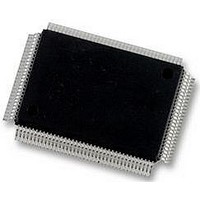
LM97593VH National Semiconductor, LM97593VH Datasheet - Page 37

LM97593VH
Manufacturer Part Number
LM97593VH
Description
12BIT ADC, 2CH, DDC/AGC, 128PQFP
Manufacturer
National Semiconductor
Datasheet
1.LM97593VH.pdf
(50 pages)
Specifications of LM97593VH
Resolution (bits)
12bit
Input Channel Type
Differential
Data Interface
Serial
Supply Voltage Range - Analogue
3V To 3.6V
Supply Voltage Range - Digital
1.6V To 2V, 3V To 3.6V
Supply
RoHS Compliant
Sampling Rate
65MSPS
Rohs Compliant
Yes
Lead Free Status / Rohs Status
Not Compliant
Available stocks
Company
Part Number
Manufacturer
Quantity
Price
Company:
Part Number:
LM97593VH/NOPB
Manufacturer:
VK
Quantity:
1 980
Company:
Part Number:
LM97593VH/NOPB
Manufacturer:
Texas Instruments
Quantity:
10 000
SFS_POL
RDY_POL
MUX_MODE
PACKED
FORMAT
FREQ_A
PHASE_A
FREQ_B
PHASE_B
A_SOURCE
B_SOURCE
EXP_INH
Reserved
Reserved
AGC_HOLD_IC
AGC_LOOP_GAIN
Reserved
AGC_IC_A
Register Name
Register Name
Width
Width
4B
2B
4B
2B
2B
1B
1b
1b
1b
1b
2b
1b
1b
1b
1b
2b
2
2
Type
Type
R/W
R/W
R/W
R/W
R/W
R/W
R/W
R/W
R/W
R/W
R/W
R/W
R/W
R/W
R/W
R/W
R/W
R/W
Default
Default
0
0
0
0
0
0
0
0
0
0
1
0
1
0
0
0
0
0
a
a
11-12
13-16
17-18
21-22
Addr
Addr
7-10
19
19
20
20
20
20
20
23
6
6
6
6
6
7:6
7:0
7:0
7:0
7:0
1:0
3:2
4:5
7:0
7:0
Bit
Bit
2
3
4
5
0
1
2
3
37
Determines polarity of the SFS output. 0=Active High. 1=Active
Low.
Determines polarity of the RDY output. 0=Active High. 1=Active
Low.
Determines the mode of the serial outputs. 0=Each channel is
output on its respective pin, 1=Both channels are multiplexed
and output on AOUT. See also .
Controls when SFS goes active. 0=SFS pulses prior to the start
of the I and the Q words. 1=SFS pulses only once prior to the
start of each I/Q sample pair (i.e. the pair is treated as a double-
sized word) The I word precedes the Q word. See .
Determines output number format. 0=Truncate serial output to
8 bits. Parallel output is truncated to 32 bits. 1=Round both serial
and parallel to 16-bits. All other bits are set to 0. 2=Round both
serial and parallel to 24-bits. All other bits are set to 0. 3=Output
floating point. 8-bit mantissa, 4-bit exponent. All other bits are
set to 0.
Frequency word for channel A. Format is a 32-bit, 2’s
complement number spread across 4 registers. The LSBs are
in the lower registers. The NCO frequency F is F/F
2
Phase word for channel A. Format is a 16-bit, unsigned
magnitude number spread across 2 registers. The LSBs are in
the lower registers. The NCO phase PHI is PHI=2*pi*PHASE_A/
2
Frequency word for channel B. Format is a 32-bit, 2’s
complement number spread across 4 registers. The LSBs are
in the lower registers. The NCO frequency F is F/F
2
Phase word for channel B. Format is a 16-bit, unsigned
magnitude number spread across 2 registers. The LSBs are in
the lower registers. The NCO phase PHI is PHI=2*pi*PHASE_B/
2
0=Select AIN as channel input source. 1=Select BIN.
2=3=Select TEST_REG as channel input source.
0=Select AIN as channel input source. 1=Select BIN.
2=3=Select TEST_REG as channel input source.
0=Allow exponent to pass into FLOAT TO FIXED converter.
1=Force exponent in DDC channel to a 7 (maximum digital
gain). This affects both channels.
AGC_FORCE on the CLC5902. Do not use.
AGC_RESET_EN on the CLC5902. Do not use.
0=Normal closed-loop operation. 1=Hold integrator at initial
condition. This affects both channels.
Bit shift value for AGC loop. Valid range is from 0 to 3. This
affects both channels.
AGC_COUNT on the CLC5902. Do not use.
AGC fixed gain for channel A. Format is an 8-bit, unsigned
magnitude number. The channel A DVGA gain will be set to the
inverted three MSBs.
32
16
32
16
.
.
.
.
Description
Description
www.national.com
CK
CK
=FREQ_A/
=FREQ_B/


